
# World's Most Powerful AI Chips: Architecture, Performance, Manufacturing Cost and Global Use
The chip that trains a large language model, the one that renders a game, and the one inside a laptop are no longer built the same way. Over the past three years, "most powerful chip" has effectively split into two questions: which chip processes the most tokens per second in a data center, and which chip does the most useful work per watt on a desk or in a pocket. This guide covers both, using the latest specifications available as of August 2026 from NVIDIA, AMD, Google, Intel, Apple and Huawei, the companies currently setting the pace in AI and high-performance silicon.
Every figure below is drawn from official specifications, company documentation, MLPerf benchmark submissions, or named industry analysts. Where a number is an estimate rather than an official disclosure, which is common for manufacturing cost, it is labeled as such.
Why Chip Architecture Matters
"Architecture" describes how a chip organizes its transistors into functional blocks, arithmetic units, memory controllers, cache, interconnect, and how those blocks talk to each other. Two chips built on the same manufacturing process can perform very differently depending on architecture. NVIDIA's Blackwell and AMD's CDNA, for instance, both use TSMC silicon, but they differ in how many low-precision math units they pack in, how memory is attached, and how multiple chips are linked into a single logical system.
For AI workloads specifically, architecture increasingly means three things: how much matrix-multiplication throughput a chip has at low numerical precision (FP8, FP4), how much fast memory sits next to the compute, and how efficiently many chips can be lashed together to act as one. A chip that wins on paper FLOPS but starves for memory bandwidth, or that scales poorly across a rack, will underperform in practice. This is why NVIDIA, AMD and Google now design GPUs and rack-scale systems together rather than as separate products.
How Semiconductor Manufacturing Affects Performance and Cost
Every chip in this guide is fabricated by TSMC, except Huawei's, which relies partly on China's SMIC. The "process node," a label like 3nm or 4nm, refers to a generation of manufacturing technology, not a literal transistor dimension. Moving to a smaller node packs more transistors into the same area and typically improves power efficiency, but it costs substantially more per wafer.
According to semiconductor cost-tracking estimates compiled from TrendForce and industry pricing data, a 300mm wafer on TSMC's mature 3nm process (N3/N3E) costs roughly $17,000–$22,000 as of mid-2026, up from about $9,500 for 7nm. TSMC's newer 2nm node (N2) is reported to run close to $30,000 per wafer, with lead times booked out to 2028. These are wafer costs only, the price of a finished chip depends heavily on die size, defect rates, and how many good chips (dies) can be cut from each wafer.
For AI accelerators specifically, the logic die itself is often the smaller part of the bill. Independent chip-cost analysis firm Epoch AI estimated in a widely cited December 2025 teardown that NVIDIA's B200 GPU costs roughly $6,400 to manufacture, and that the logic die accounts for less than 15% of that figure. High-bandwidth memory (HBM) makes up nearly half the cost, with advanced packaging adding most of the rest. That balance, in which memory and packaging costing more than the processor itself, is now typical across the AI accelerator market and is the reason HBM supply has become as strategically important as the chips themselves.
The Role of Advanced Packaging, HBM and Chiplets
Three interlinked technologies explain most of what separates a modern AI chip from a chip built five years ago.
High-Bandwidth Memory (HBM) stacks multiple DRAM dies vertically and connects them to the processor through thousands of short, wide electrical connections, rather than the handful of pins used by conventional memory. This gives AI chips terabytes-per-second of bandwidth rather than the hundreds of gigabytes per second typical of PC memory. HBM is manufactured almost exclusively by SK hynix and Samsung, with Micron a smaller third supplier. Estimated per-stack pricing has risen with each generation: roughly $200 for a 24GB HBM3 stack, climbing toward an estimated $500 for a 48GB HBM4 stack, according to semiconductor market-data trackers. HBM4, now entering production, roughly doubles per-pin data rates over HBM3E and is the memory standard underpinning NVIDIA's Rubin and AMD's MI400 generations.
Chiplets break a single large chip into several smaller dies that are then bonded together in one package. Smaller dies have higher manufacturing yield, fewer defects per die, which matters because defect rates rise sharply with die area. AMD's MI455X, for example, combines twelve separate compute and I/O dies rather than one monolithic chip. The tradeoff is packaging cost and complexity: connecting chiplets requires the third piece of this puzzle.
Advanced packaging, TSMC's CoWoS (Chip-on-Wafer-on-Substrate) process, Intel's EMIB, and 3D-stacking techniques like SoIC, is what physically joins compute dies to HBM stacks and to each other. CoWoS-L packaging and assembly can add roughly $700–$1,000 to the cost of a single AI accelerator package, according to cost-modeling firm Silicon Analysts, and TSMC's CoWoS capacity has been reported as fully booked through 2026, with NVIDIA alone estimated to hold around 60% of it. This packaging bottleneck, more than raw wafer supply, is currently one of the tightest constraints on how many high-end AI chips can reach the market.
NVIDIA: Blackwell Ultra (B300 / GB300) and the Rubin Transition
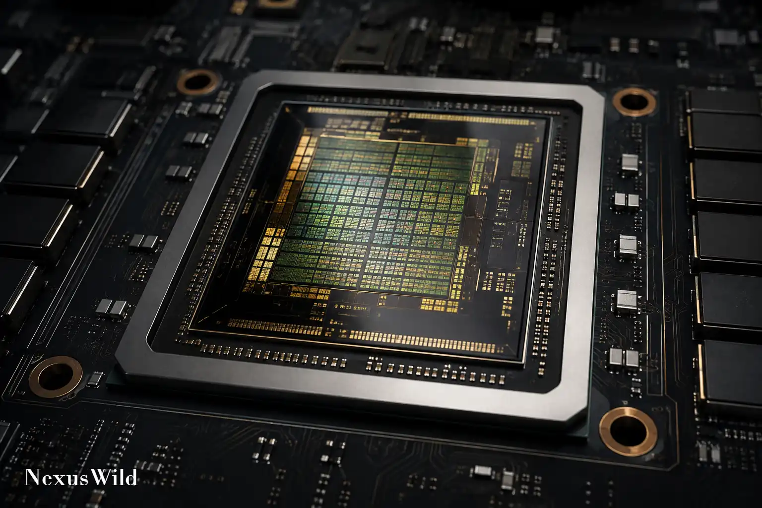
Architecture and process. NVIDIA's current flagship data-center GPU is Blackwell Ultra, sold as the standalone B300 GPU or as part of the GB300 Grace Blackwell Ultra superchip, which pairs two B300 dies with a 72-core Arm-based Grace CPU. The underlying Blackwell die family is fabricated on a custom TSMC process NVIDIA calls "4NP," a refined 4-nanometer-class node. NVIDIA's earlier B200 GPU was disclosed at 208 billion transistors; NVIDIA has not published a separate transistor count for the B300 revision.
Memory and bandwidth. The B300 carries 288GB of HBM3e memory, up from 192GB on the original B200, with per-GPU bandwidth reported at roughly 8 TB/s (some system documentation citing aggregate figures above 10 TB/s as memory stacking configurations vary). NVLink 6 provides up to 1.8 TB/s of GPU-to-GPU bandwidth.
Compute and benchmarks. NVIDIA cites roughly 15 petaFLOPS of dense FP4 compute per GPU. At the system level, an 8-GPU DGX B300 is rated by NVIDIA at 192 petaFLOPS for inference and 70 petaFLOPS for training. In MLPerf Inference v6.0 (April 2026), the industry's standard benchmark suite, systems built on Blackwell Ultra recorded the highest throughput across the widest range of models and scenarios of any submission, per MLCommons results cited by NVIDIA.
Power. Up to 1,400W per GPU in liquid-cooled rack configurations, according to Supermicro and AceCloud system documentation, a power level that makes air cooling impractical.
Manufacturing cost. No official cost has been published for the B300. Epoch AI's independent teardown of the smaller-memory B200 estimated a manufacturing cost of about $6,400, with HBM alone accounting for roughly $2,900 and advanced packaging around $1,100. Because the B300 carries 50% more HBM, its true manufacturing cost is almost certainly higher, though no independent breakdown has been published as of this writing. Market pricing for a standalone B300 GPU was reported around $53,000 in July 2026 by GPU cloud provider Spheron Network; a full liquid-cooled GB300 NVL72 rack is estimated in the $3–4 million range by industry trackers, an estimate, not a published NVIDIA price.
Manufacturing partners. TSMC fabricates the logic dies and performs CoWoS-L packaging; HBM3e is supplied primarily by SK hynix, with Samsung and Micron as secondary sources.
Use cases and global deployment. Blackwell Ultra systems are deployed by every major hyperscaler, AWS, Microsoft Azure, Google Cloud, Oracle Cloud, plus specialist GPU clouds such as CoreWeave, for large language model training, inference, and agentic AI workloads. NVIDIA's Blackwell architecture also underpins its GeForce RTX 50-series gaming GPUs, a separate consumer product line built on related but distinct silicon. Export controls restrict sales of NVIDIA's most capable data-center chips to China, a policy area that has directly benefited Huawei's domestic alternatives (see below).
Advantages and limitations. Blackwell Ultra's advantages are the CUDA software ecosystem, the broadest MLPerf benchmark coverage of any accelerator, and the highest per-GPU memory bandwidth on the market. Its limitations are cost, power density that requires liquid cooling infrastructure most data centers still lack, and dependence on CoWoS packaging capacity that is fully booked industry-wide.
What comes next. NVIDIA's Rubin architecture, built around the R100 GPU, entered full production in early 2026 and is expected to reach cloud providers including Microsoft, AWS and Google Cloud in the second half of the year. Rubin moves to a TSMC 3nm process, pairs a 336-billion-transistor GPU die with a new 227-billion-transistor Vera CPU (successor to Grace), and switches to HBM4, 288GB per GPU at up to 22 TB/s, according to NVIDIA's GTC 2026 disclosures and independent analysis from Thunder Compute. NVIDIA states Rubin will deliver roughly 50 petaFLOPS of dense FP4 compute per GPU, with a "Rubin Ultra" variant doubling that to 100 petaFLOPS expected in 2027.
AMD: Instinct MI355X and the MI400 Series
Architecture and process. AMD's currently shipping flagship, the Instinct MI355X (available since June 2025), uses AMD's CDNA-based architecture manufactured on TSMC's advanced nodes. Each MI355X module carries 288GB of HBM3E and 8.0 TB/s of memory bandwidth, according to AMD's own platform datasheet; an 8-GPU MI355X platform delivers a rated 80.5 petaFLOPS of peak MXFP4 matrix compute in aggregate, roughly 10 petaFLOPS per GPU.
AMD's next generation, the Instinct MI400 series, launched at CES 2026 and is entering production through the year. Its flagship, the MI455X, uses AMD's CDNA 5 architecture built as a chiplet design: twelve compute and I/O dies combining TSMC's N2 (2nm) and N3 (3nm) processes, totaling roughly 320 billion transistors, per AMD's own product briefing.
Memory and bandwidth. The MI455X carries 432GB of HBM4, the largest memory capacity of any AI accelerator covered here, with up to 23.3 TB/s of bandwidth, according to AMD's datasheet.
Compute and benchmarks. AMD rates the MI455X at up to 40 petaFLOPS of FP4 compute and 20 petaFLOPS at FP8. A full AMD Helios rack, 72 MI455X GPUs, is rated at up to 2.9 exaFLOPS of FP4 and 1.4 exaFLOPS of FP8 compute, with 31TB of aggregate HBM4 and 1.67 PB/s of memory bandwidth across the rack.
Power and manufacturing cost. AMD has not published per-GPU TDP figures for the MI455X in its public materials reviewed here. No independent, publicly verified manufacturing-cost teardown comparable to Epoch AI's NVIDIA analysis exists for AMD's Instinct line at the time of writing; industry margin estimates place AMD's data-center GPU gross margins around 65–70%, below NVIDIA's estimated 80%+, reflecting AMD's more price-competitive positioning.
Manufacturing partners. TSMC fabricates both the MI355X and MI455X, with HBM supplied by SK hynix and Samsung.
Use cases and global deployment. AMD positions the MI400 family across three variants: the MI455X and MI450X for large-scale AI training and inference, and the MI430X for scientific and sovereign-AI computing, where it delivers up to 288 teraFLOPS of hardware FP64 performance, a precision level AI-focused chips typically don't optimize for. AMD has reported growing customer interest from major AI labs and hyperscalers alongside its established base of cloud and government HPC customers, using the open ROCm software stack and standards-based Ethernet and UALink interconnects rather than a proprietary alternative to NVLink.
Advantages and limitations. AMD's chips offer the largest per-GPU memory capacity in this comparison, an important advantage for memory-constrained "mixture of experts" models, and an open interconnect and software stack. The tradeoff is a less mature software ecosystem than CUDA, which historically has meant more engineering effort to reach peak utilization, and a smaller base of third-party tooling and pre-optimized models.
Google: TPU v7 "Ironwood"
Google's Tensor Processing Units are custom accelerators, designed in-house and manufactured for Google's exclusive use, they are never sold as discrete hardware and are accessible only through Google Cloud.
Architecture. Ironwood (TPU v7, also referred to as TPU7x) is Google's seventh-generation TPU and its first designed with native FP8 support. Each chip contains two TensorCores and four SparseCores, the latter specialized for handling embeddings in recommendation and ranking workloads. Google has not disclosed the manufacturing process node publicly.
Memory and compute. According to Google Cloud's own documentation, each Ironwood chip carries 192GB of HBM3e memory with roughly 7.4 TB/s of bandwidth, up sharply from the 95GB on the prior TPU v5p generation. Peak compute is rated at 2,307 teraFLOPS in BF16 and 4,614 teraFLOPS in dense FP8 per chip, a figure independent analysis from SemiAnalysis notes is slightly ahead of NVIDIA's B200 at the same precision.
Power. Google has not published an official TDP for Ironwood. Based on the company's disclosure that a 9,216-chip liquid-cooled pod draws close to 10 megawatts, industry analysis at XPU.pub estimates roughly 1 kilowatt per chip, an estimate, not a Google-confirmed figure.
Scale. Ironwood chips interconnect at 1.2 TB/s per chip and scale to pods of up to 9,216 chips, connected through Google's optical circuit switching network.
Manufacturing cost. Not disclosed and not independently estimated in any credible public source identified for this guide, reflecting the fact that TPUs are never sold as standalone units with a market price.
Use cases and global deployment. Ironwood powers Google's own Gemini models and is reported by industry analysts to be used by outside AI labs including Anthropic, which has committed to large-scale TPU capacity, alongside other Google Cloud AI customers. It is deployed within Google's own data center regions worldwide rather than sold to enterprises for on-premises use.
Advantages and limitations. Ironwood's tight integration with Google's software stack (JAX, XLA) and its FP8 performance parity with NVIDIA's Blackwell generation are genuine strengths, achieved roughly a year after Blackwell's own availability. Its main limitation is accessibility: it cannot be purchased or run outside Google Cloud, unlike GPU-based alternatives.
Intel: Gaudi 3 and Crescent Island
Gaudi 3: Current Generation Intel's Gaudi 3 accelerator, manufactured on TSMC's 5-nanometer (N5) process, carries 128GB of HBM2e memory with 3.7 TB/s of bandwidth and delivers a rated 1.8 petaFLOPS of FP8/BF16 compute, per Intel's own white paper. It draws up to 900W air-cooled or 1,200W liquid-cooled and uses standard Ethernet networking (24 ports of 200GbE) rather than a proprietary interconnect, a deliberate design choice to avoid lock-in to NVIDIA's NVLink/InfiniBand ecosystem. Third-party deployment analysis has estimated Gaudi 3 pricing around $15,000 per accelerator, roughly half of contemporaneous H100 pricing, though this figure is a market estimate rather than an Intel list price.
Status. Gaudi has struggled commercially: Intel missed its own 2024 revenue target for the product line, and the company has signaled it will wind down Gaudi in 2026–2027 in favor of newer architectures.
Crescent Island: Upcoming Announced in late 2025, Crescent Island is Intel's next data-center GPU, built on the "Xe3P" architecture, a performance-tuned version of the Xe3 graphics architecture used in Intel's Panther Lake client chips. It targets air-cooled enterprise inference servers, pairs with 160GB of LPDDR5X memory rather than HBM (a cost and simplicity tradeoff), and is expected to reach customer samples in the second half of 2026. Beyond Crescent Island, Intel has reportedly shelved its Falcon Shores AI chip commercially in favor of a further successor, code-named Jaguar Shores, built on Intel's own 18A process node and slated for late 2026.
Manufacturing partners. Gaudi 3 is fabricated by TSMC (N5); Crescent Island's foundry has not been publicly confirmed at the time of writing.
Use cases and global deployment. Intel has positioned Gaudi 3 primarily for enterprise LLM inference and retrieval-augmented generation (RAG) workloads, and has even integrated Gaudi racks with NVIDIA Blackwell hardware in disaggregated inference designs, using Blackwell GPUs for the compute-heavy "prefill" stage and Gaudi for the memory-bound "decode" stage, an unusual example of direct interoperability between competing accelerator families.
Advantages and limitations. Gaudi's standard-Ethernet networking and lower price point are genuine differentiators for cost-sensitive deployments, but its software ecosystem lags CUDA and ROCm, it currently lacks support for tools like RAPIDS and NVIDIA's Triton Inference Server, and its commercial traction has been limited compared to NVIDIA and AMD.
Huawei: Ascend 910C and the Domestic Alternative
Context. Huawei's Ascend line exists largely because of US export controls that block NVIDIA's most capable AI chips from sale in China. It is the leading domestic alternative for Chinese AI developers.
Architecture and process. The Ascend 910C is a dual-die chiplet design built on a roughly 7-nanometer-class process. Reporting from SemiAnalysis and The Register indicates a substantial share of the chip's compute dies were originally fabricated by TSMC and obtained through third-party channels before restrictions tightened further; China's SMIC, which lacks access to EUV lithography and instead relies on older deep-ultraviolet tools with multi-patterning, also produces 7nm-class ("N+2") chips for Huawei domestically.
Memory and compute. Each 910C carries 128GB of HBM2e memory with 3.2 TB/s of bandwidth (split across two compute dies at 1.6 TB/s each), and delivers roughly 750–780 teraFLOPS of dense BF16/FP16 compute, according to teardown analysis published by The Register. The chip does not natively support FP8, a precision format central to NVIDIA and Google's newest chips, relying instead on INT8. Chip-to-chip interconnect bandwidth is rated at 540 GB/s bidirectional.
Scale-out approach. Rather than compete chip-for-chip, Huawei scales out: its CloudMatrix 384 rack-scale system links 384 Ascend 910C chips across 16 racks using an all-optical interconnect. The Register's analysis found this system delivers about 60% higher dense FP16 compute and roughly double the memory bandwidth of an NVIDIA GB200 NVL72 rack, but achieves that by using more than five times as many accelerators across sixteen times the floor space, at an estimated 2.3x worse performance-per-watt.
Production. Huawei reportedly plans to manufacture around 600,000 Ascend 910C dies in 2026, roughly double 2025 output, according to Bloomberg reporting citing people familiar with the matter.
Manufacturing cost. No credible independent cost estimate was identified for this guide; Huawei does not publish pricing, and the mixed TSMC/SMIC sourcing history makes standard cost-modeling approaches unreliable.
Use cases and global deployment. Ascend chips are used almost exclusively within China, by companies including Alibaba and DeepSeek, along with state-linked infrastructure projects, as a substitute for restricted NVIDIA hardware.
What comes next. Huawei's successor Ascend 910D is targeting performance beyond NVIDIA's H100, and the company has announced an Ascend 950 series, the 950PR and 950DT variants, for 2026, notable for using Huawei's own in-house HBM designs (HiBL 1.0 and HiZQ2.0) rather than the SK hynix or Samsung memory used by every other chip in this guide, a step toward memory self-sufficiency alongside logic self-sufficiency.
Apple: M5: AI Compute at the Edge
Apple's M5 belongs to a different category from the chips above: it is a consumer system-on-chip for Macs and iPads, optimized for power efficiency and on-device AI rather than data-center throughput. It is included here because "most powerful chips" increasingly includes the silicon running AI locally on personal devices, not only in the cloud.
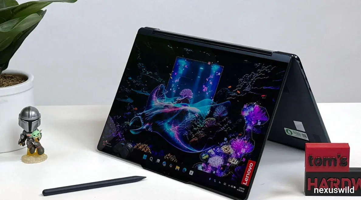
Architecture and process. The M5, Apple's fifth-generation Apple Silicon chip, launched in 2026 on TSMC's 3-nanometer N3P process (a refined variant of the N3 node; some analysis suggests the base M5 die specifically uses the closely related N3E node, with Pro and Max variants confirmed on N3P). It integrates an 8-core CPU (4 performance + 4 efficiency cores), a 10-core GPU with dedicated Neural Accelerators built into each GPU core, and a 16-core Neural Engine, all sharing a single unified memory pool.
Memory. 16GB of unified LPDDR5X memory as the new base configuration, up from 8GB on the M4, with bandwidth reported in the range of roughly 120–153 GB/s depending on source and configuration.
Performance. Apple and independent reviewers report gains over the M4 of roughly 15–20% for CPU tasks, 25–30% for GPU tasks, and 30–40% for Neural Engine (AI) workloads, driven primarily by the new per-core GPU Neural Accelerators rather than a large jump in transistor count.
Manufacturing cost. Apple does not disclose chip manufacturing costs. TSMC's N3P wafers are estimated at roughly $16,000 each, compared with an estimated $20,000+ for TSMC's 2nm node, a cost gap analysts have cited as a reason Apple stayed on 3nm for the M5 generation rather than moving immediately to N2.
Manufacturing partners. TSMC exclusively, using the same N3-family process across the entire M5 rollout, which spans MacBook Pro, MacBook Air, iPad Pro, Mac mini and Mac Studio through 2026.
Use cases and global deployment. The M5 targets consumer and prosumer computing, video and photo editing, on-device generative AI features (Apple Intelligence), local inference for small language models, and general productivity, sold globally through Apple's retail and enterprise channels.
Advantages and limitations. The M5's unified memory architecture and power efficiency remain distinctive relative to competing laptop chips, and its per-core GPU AI accelerators are a genuine architectural change from the M4. But its raw compute, memory bandwidth and capacity are, by design, far below any data-center accelerator, it is not intended for large-scale model training, and Apple's single-vendor, closed hardware-software ecosystem is itself a constraint for some buyers.
Comparing the Data-Center AI Accelerators
The table below focuses on chips built for AI training and inference in data centers. Apple's M5 is excluded here since it serves a fundamentally different market (personal computing rather than data-center throughput); figures for chips still ramping to volume production in 2026 (Rubin R100, MI455X, Crescent Island) reflect announced specifications rather than shipped-product benchmarks.
| Chip Company Process Node Memory Bandwidth Peak Low-Precision Compute TDP Est. Manufacturing Cost | |||||||
|---|---|---|---|---|---|---|---|
| Blackwell Ultra (B300) | NVIDIA | TSMC 4NP (\~4nm-class) | 288GB HBM3e | \~8 TB/s | \~15 PFLOPS (dense FP4, per GPU) | Up to 1,400W | Not disclosed; B200 (192GB variant) estimated at \~$6,400 by Epoch AI |
| Rubin (R100)\* | NVIDIA | TSMC N3 (3nm) | 288GB HBM4 | Up to 22 TB/s | \~50 PFLOPS (dense FP4) | Not disclosed | Not disclosed |
| Instinct MI355X | AMD | TSMC advanced node (undisclosed by AMD) | 288GB HBM3E | 8.0 TB/s | \~10 PFLOPS (MXFP4, per GPU) | Not disclosed | Not independently estimated |
| Instinct MI455X\* | AMD | TSMC N2 + N3 (chiplet) | 432GB HBM4 | 23.3 TB/s | 40 PFLOPS (FP4) | Not disclosed | Not independently estimated |
| TPU v7 "Ironwood" | Not disclosed | 192GB HBM3e | 7.4 TB/s | 4,614 TFLOPS (dense FP8) | \~1kW (estimated) | Not applicable (not sold) | |
| Gaudi 3 | Intel | TSMC N5 (5nm) | 128GB HBM2e | 3.7 TB/s | 1.8 PFLOPS (FP8/BF16) | 900W air / 1,200W liquid | \~$15,000 sale price (reported estimate; manufacturing cost not disclosed) |
| Ascend 910C | Huawei | \~7nm-class (SMIC/TSMC) | 128GB HBM2e | 3.2 TB/s | \~0.75–0.78 PFLOPS (dense BF16/FP16) | Not disclosed | Not independently estimated |
\*Ramping to volume production/shipment during 2026; specifications reflect vendor announcements rather than shipped-hardware benchmarks.
No single chip in this table is unambiguously "most powerful", it depends on the metric. NVIDIA's Rubin leads on announced peak FP4 throughput and memory bandwidth once it ships at volume. AMD's MI455X leads on raw memory capacity, an advantage for the largest mixture-of-experts models. Google's Ironwood leads on FP8 throughput per chip among currently-shipping hardware. Huawei's Ascend 910C trails every other chip here on a per-unit basis but is deployed at far larger cluster scale to compensate, a strategy shaped directly by manufacturing access rather than architectural choice.
Why Taiwan, South Korea, the US and Other Regions Matter
Taiwan is the center of gravity for advanced chip manufacturing. TSMC alone is estimated to account for the large majority of the world's most advanced logic chip production and, according to its own regulatory filings, deployed over 300 distinct process technologies for more than 500 customers in 2025. Every chip covered in this guide except Huawei's is fabricated primarily by TSMC, including chips designed by companies headquartered in the US, and TSMC's advanced packaging lines (CoWoS) are currently a tighter bottleneck on AI chip supply than wafer capacity itself.
South Korea dominates the memory side of the equation. SK hynix and Samsung together supply the overwhelming majority of the HBM that feeds every major AI accelerator; SK hynix has been reported as the first supplier sampling HBM4 to its lead customer. This gives South Korea outsized leverage over how many AI chips can actually reach the market, independent of logic fab capacity.
The United States houses the design and IP layer: NVIDIA, AMD, Google, Intel and Apple are all US-headquartered, and US export-control policy directly shapes where advanced chips can be sold, most visibly in the restrictions that have pushed Chinese developers toward Huawei's domestic Ascend line. Intel remains the only US-headquartered company manufacturing leading-edge logic domestically, though it trails TSMC on the most advanced nodes.
Other regions matter further up the supply chain: the Netherlands, through ASML, is the sole global source of the extreme ultraviolet (EUV) lithography machines required for any 5nm-or-below chip, a dependency that underlies China's inability to match TSMC's process capability. Japan supplies critical semiconductor materials and some lithography and inspection equipment. China, blocked from EUV access, has built a domestic ecosystem around SMIC's mature-node DUV processes, sufficient for 7nm-class chips like the Ascend 910C but not yet for the 3nm and 2nm nodes NVIDIA and AMD now use.
The Current Competition in AI and High-Performance Computing
Three dynamics currently define competition among these chipmakers.
Training versus inference specialization. Early AI chip competition centered on training, building ever-larger models. As deployment has scaled, inference (running trained models for users) has become the larger and more cost-sensitive workload, which is why Intel, AMD and Google have all emphasized inference-optimized designs (Crescent Island, and Ironwood's native FP8 support) alongside their training hardware.
Software ecosystem as a moat. NVIDIA's CUDA software stack remains the primary reason its hardware commands premium pricing and margins despite competitors sometimes matching or exceeding it on paper specifications. AMD's ROCm and Google's JAX/XLA are both maturing alternatives, but switching costs, re-optimizing models and infrastructure, remain a real barrier for large AI labs.
Supply constraints and export policy. HBM and CoWoS packaging capacity, not wafer supply, are the binding constraints on how fast the industry can ship new AI chips, with NVIDIA reported to hold roughly 60% of global CoWoS capacity. Simultaneously, US export controls on advanced chips to China have accelerated Huawei's independent chip and HBM development, a geopolitical dynamic likely to keep shaping two increasingly separate AI hardware ecosystems, one built on TSMC-manufactured Western chips and one built on domestic Chinese fabrication, for the foreseeable future.
Figures in this article reflect publicly available specifications, official vendor documentation, MLPerf benchmark results, and named industry analysis (including Epoch AI, SemiAnalysis, TrendForce-sourced pricing data, and Silicon Analysts cost modeling) as of August 2026. Manufacturing costs, transistor counts and power figures are explicitly labeled as estimates where no official disclosure exists; several chips discussed (NVIDIA Rubin, AMD MI455X, Intel Crescent Island) were entering production or ramping to volume shipment at the time of writing, and their real-world benchmark performance may differ from announced specifications.
Reader questions
Frequently asked questions
What is the most powerful AI chip in 2026?
There is no single answer because performance depends on the workload and precision. NVIDIA Rubin leads on announced FP4 throughput, while AMD MI455X has the largest stated memory capacity among the accelerators compared in this guide.
Why is HBM important for AI chips?
High-bandwidth memory delivers the bandwidth needed to keep large AI models supplied with data. Its cost and availability have become central constraints for advanced AI accelerator production.
What is advanced packaging in AI hardware?
Advanced packaging connects logic dies, chiplets and HBM stacks within one package. Technologies such as TSMC CoWoS allow much wider, faster links than conventional chip packaging.
Can Google TPU Ironwood be bought as a chip?
No. Google designs TPU Ironwood for use through Google Cloud and does not sell it as a standalone accelerator.
Why does NVIDIA retain an advantage in AI chips?
NVIDIA combines high-performance hardware with CUDA, a mature software ecosystem, broad tooling and large-scale systems integration, which can reduce deployment and optimization effort for customers.
Nexuswild welcomes factual corrections. Email contact@nexuswild.com with evidence and the article URL.