
Making transistors smaller used to be enough. Shrink the feature size, cram more logic onto a die, and performance climbed almost automatically. That formula still works, but it's getting slower, harder and far more expensive with each generation, which is why so much of the industry's energy right now is going into something less flashy than the next process node: how chips are packaged together.
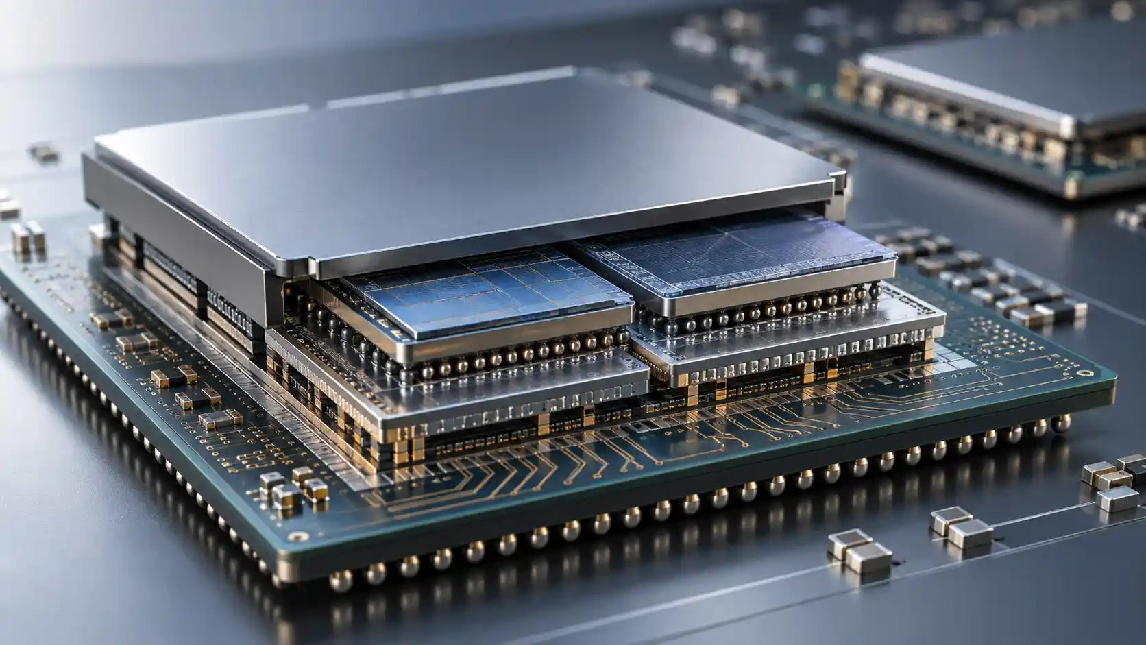
Advanced packaging, at its simplest, is the art of combining multiple pieces of silicon, sometimes different chips entirely, into one finished unit that behaves like a single, more capable chip. Two approaches dominate today. In 2.5D packaging, several dies sit side by side on a shared base called an interposer, wired together for fast, high-bandwidth communication; TSMC's CoWoS platform is the best-known commercial example. In 3D packaging, dies are stacked vertically instead, shortening the distance signals have to travel, as in TSMC's SoIC or Intel's Foveros Direct. Increasingly, chipmakers combine both in a single package, an approach the industry calls 3.5D, which is exactly how AMD's MI300 accelerator pairs stacked compute dies with high-bandwidth memory.
Chiplets are the other half of this story: instead of building one enormous, expensive-to-manufacture die, designers now build a system from several smaller, specialized dies, and stitch them together. A shared industry standard called UCIe is meant to let chiplets from different companies talk to each other, which matters because no single company can efficiently make every part of a modern AI chip.
The technique making finer chip-to-chip connections possible is hybrid bonding, which joins copper pads directly, chip to chip, without the solder bumps older packaging methods relied on. It's already in high-volume commercial use for logic-to-logic stacking, AMD's latest 3D V-Cache uses it at a 9-micron pitch, which the company says delivers a tenfold bandwidth improvement over conventional packaging, though applying the same technique to memory stacking has reportedly been delayed. Worth noting: there's a real gap between the lab and the factory floor here. TSMC's commercial hybrid bonding currently sits around 6 microns, while research groups like imec and EV Group demonstrated a 200-nanometer pitch on a test wafer earlier this year. That's promising, but it's a research result, not something shipping in a product yet.
None of this is happening in a vacuum. AI accelerators are the reason packaging suddenly matters so much, because they need to pair compute dies with as much high-bandwidth memory as possible, and demand for that memory is currently outstripping supply. TSMC has been scaling its CoWoS capacity aggressively as a result, from roughly 13,000 wafers a month in 2023 toward a target in the range of 100,000 to 120,000 wafers monthly, alongside a new, dedicated advanced-packaging campus in Chiayi, Taiwan.
Other major players are carving out their own space. Samsung has its own hybrid-bonding platform for stacking memory and chiplets, Intel is pushing its own 3D approach, and assembly specialists like ASE and Amkor handle packaging for companies that don't own their own advanced fabs. Bloomberg Intelligence has projected the advanced packaging market could grow roughly eightfold, to around $80 billion, by 2033, though that's a forecast, not a guarantee.
It's worth being clear about what packaging isn't: a replacement for shrinking transistors. It's a complement, a way to keep extracting performance gains even as traditional scaling slows down, by getting smarter about how chips are put together rather than just how small they can be made.
Further reading and useful links
Reader questions
Frequently asked questions
What is advanced semiconductor packaging?
Advanced packaging is the method of combining multiple pieces of silicon or specialized chiplets into a single unified package using technologies like 2.5D interposers and 3D vertical stacking.
What is the difference between 2.5D and 3D packaging?
In 2.5D packaging, dies sit side-by-side on a shared base or interposer (such as TSMC's CoWoS), whereas in 3D packaging, dies are stacked directly on top of each other vertically.
Why is advanced packaging becoming so important for AI chips?
AI accelerators require compute dies to be tightly coupled with large amounts of high-bandwidth memory, making advanced packaging essential for high-speed data transfer and overcoming traditional transistor scaling limits.
What role does hybrid bonding play in advanced packaging?
Hybrid bonding directly joins copper pads chip-to-chip without traditional solder bumps, dramatically improving bandwidth and connection density between stacked dies.
Nexuswild welcomes factual corrections. Email [email protected] with evidence and the article URL.