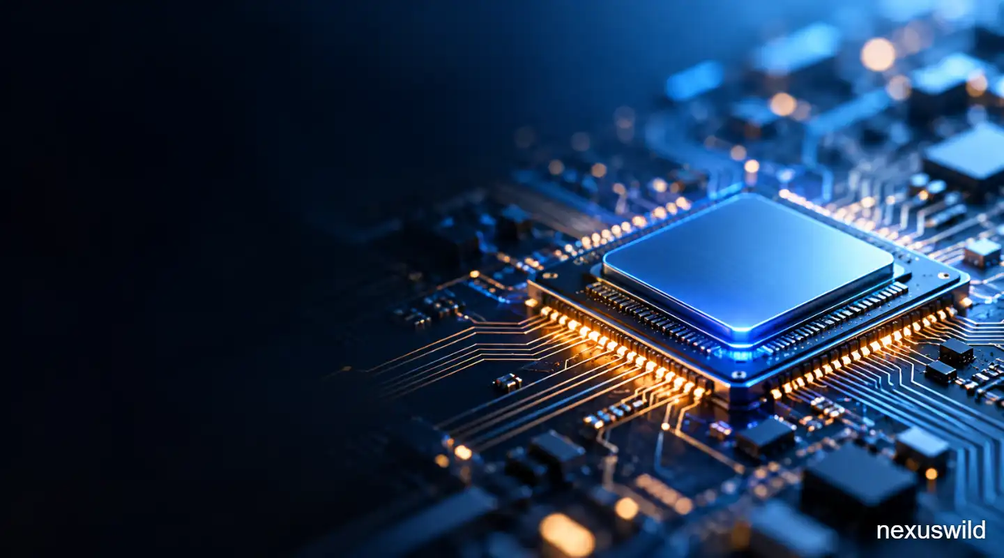

For decades, progress in chips could be explained largely through smaller process nodes: fit more transistors onto a piece of silicon, improve performance and reduce power consumption. That formula still matters, but it is becoming only one part of a much larger engineering problem.
Today's highest-performance processors increasingly combine gate-all-around transistors, chiplets, advanced packaging, vertically stacked dies and high-bandwidth memory. At the same time, researchers are testing new semiconductor materials that could eventually extend scaling beyond conventional silicon.
The result is a change in both chip architecture and the industrial structure behind it. Foundries, memory manufacturers, packaging companies and materials specialists are becoming more tightly connected, while advanced packaging and memory are emerging as strategic capabilities alongside leading-edge wafer fabrication.
Advanced Nodes Are Changing Internally, Not Just Getting Smaller
The transition to the 2-nanometre generation illustrates how semiconductor scaling itself is changing.
TSMC began volume production of its N2 process in the fourth quarter of 2025. Unlike its earlier 3nm technology, N2 uses nanosheet gate-all-around transistors, in which the gate surrounds the channel more completely to improve control of electrical current as transistors shrink.
Samsung has also moved its second-generation 2nm SF2 process into mass production, building on the gate-all-around architecture it introduced at 3nm. Samsung says SF2 is intended for mobile, AI, high-performance computing and eventually automotive applications.
Intel is approaching the same problem with its 18A process. The technology entered production in 2025 and combines Intel's RibbonFET gate-all-around transistor architecture with PowerVia, which moves power delivery to the back of the wafer. Intel's enhanced 18A-P process entered risk production in June 2026.
Backside power is becoming increasingly important because modern chips have to route both data signals and electricity through extraordinarily dense wiring networks.
TSMC's A16 process, planned around its Super Power Rail backside-power technology, similarly separates power delivery from much of the front-side signal routing. TSMC says A16 is designed particularly for high-performance computing where dense logic makes power distribution difficult.
The shift shows why node names alone now tell less of the story. Transistor structure and power delivery have become almost as important as nominal feature size.
Chiplets Are Replacing the Idea of One Giant Chip
Another major change is architectural.
Rather than building every function on a single enormous piece of silicon, chip designers are increasingly dividing processors into smaller chiplets and connecting them inside one package.
This allows different functions to be manufactured on the process technology best suited to them. High-performance compute cores might use an advanced node, while I/O or cache dies can sometimes use older and less expensive processes.
AMD has made chiplet design central to its data-centre products. Its current CDNA architecture divides compute, memory, cache and I/O functions across specialised dies. The company's MI455X AI accelerator uses multiple 3D-connected compute chiplets together with HBM4 memory.
Industry standards are also developing around this model.
The Universal Chiplet Interconnect Express, or UCIe, specification provides a common framework for connecting chiplets. UCIe 3.0, released in August 2025, supports data rates up to 64 GT/s, while the earlier UCIe 2.0 specification added support for 3D chiplet systems.
Open interconnect standards could eventually make it easier to combine dies from different suppliers, although truly interchangeable multi-vendor chiplets remain an industry goal rather than a universal reality today.
Advanced Packaging Has Become a Core Computing Technology
Once a processor is split into chiplets, connecting those pieces becomes critical.
That is why packaging, once treated as a relatively late and less glamorous manufacturing step, is becoming one of the most important areas of semiconductor technology.
TSMC's CoWoS platform places processors and high-bandwidth memory together on advanced interposers. The company began producing 5.5-reticle-size CoWoS systems in 2026, allowing significantly larger packages for AI and high-performance computing.
TSMC's SoIC technology goes further by vertically stacking silicon dies. Its 3nm SoIC chip-on-wafer technology entered volume production in 2025.
Intel's Foveros platform and Samsung's X-Cube and I-Cube technologies reflect the same broader trend: performance is increasingly being gained by integrating chips vertically or side by side rather than relying exclusively on a single monolithic die.
This changes the economics of semiconductor manufacturing. A leading-edge fab is still essential, but possessing the ability to package many complex dies together efficiently is becoming another competitive advantage.
HBM Has Become Almost as Important as the AI Processor
Artificial-intelligence systems have made memory bandwidth one of the industry's biggest engineering constraints.
AI accelerators need to move enormous quantities of data between processors and memory. Traditional DRAM placed farther away on a circuit board cannot provide enough bandwidth efficiently for the largest workloads.
High-bandwidth memory, or HBM, solves part of that problem by stacking DRAM dies vertically and placing them close to the processor.
The industry is now moving into HBM4.
SK hynix said it began mass shipments of HBM4 during the second quarter of 2026. Micron says its 36GB 12-layer HBM4 is in high-volume production, delivering more than 2.8 terabytes per second of bandwidth per stack.
Samsung has also moved HBM4 into mass production and in May 2026 began shipping HBM4E samples to major customers.
These developments help explain why the competitive landscape in AI hardware extends well beyond GPU design.
The performance of an AI accelerator now depends on the processor, memory, interconnect and package working as a tightly integrated system.
3D Integration Is Turning Chips Into Systems
The next step is increasingly three-dimensional.
Instead of placing dies only next to one another, manufacturers are stacking logic, cache and other functions vertically using extremely dense connections.
AMD's current CDNA 5 design, for example, uses 3D hybrid-bonded compute dies, while TSMC's SoIC platform supports chip-on-wafer and wafer-on-wafer stacking.
Shorter connections can reduce the distance that data must travel, improving bandwidth and potentially lowering energy use.
But 3D integration introduces another problem: heat.
Stacking active silicon makes thermal management harder. That means packaging technology, cooling systems and power delivery increasingly have to be designed together with the processor itself.
For data centres, this system-level engineering is becoming as important as raw transistor density.
Automotive Chips Are Moving Toward More Advanced Processes
Cars are another part of the semiconductor market affected by the shift.
Modern vehicles require processors for driver-assistance systems, infotainment, cameras, radar, power management and increasingly AI workloads.
TSMC says automotive products using its N5A automotive-grade 5nm process entered volume production in 2025, while its N4A automotive process is scheduled to become ready by the end of 2026.
Samsung has also been extending its gate-all-around roadmap toward automotive applications.
Yet automotive semiconductor manufacturing cannot simply copy the consumer-electronics industry. Vehicle chips typically need longer product lifetimes and demanding reliability qualifications, meaning mature nodes will remain important even as more advanced processors enter cars.
The industry's future will therefore involve a mixture of cutting-edge AI processors and much older but highly dependable power, sensor and control chips.
New Materials Could Extend Scaling, but Much of the Work Is Still Experimental
Silicon itself is also being pushed toward physical limits.
Researchers are investigating atomically thin materials such as molybdenum disulfide, tungsten disulfide and tungsten diselenide for future transistor channels.
In June 2026, research institute imec, working with TSMC and ASML, demonstrated n-type and p-type transistors using two-dimensional materials on a 300mm wafer integration platform. The work included MoS₂ and WS₂ or WSe₂ channels.
That is an important research milestone, but it is not a commercial manufacturing announcement.
Imec itself says significant development is still required before 2D-material transistors can enter industrial production.
This is a useful reminder that semiconductor research roadmaps extend far beyond technologies currently appearing in products.
The Supply Chain Is Being Redrawn Around More Than Fabs
These technological changes are also altering semiconductor geopolitics.
Countries once focused primarily on attracting wafer fabrication plants. Increasingly, they are also investing in packaging, substrates and related materials.
The United States awarded $1.4 billion in funding under its National Advanced Packaging Manufacturing Program in January 2025, explicitly aiming to develop domestic advanced-packaging capabilities.
Europe's proposed Chips Act 2.0, presented in June 2026, similarly focuses on reducing strategic dependencies while supporting more advanced semiconductor production.
TSMC, meanwhile, continues expanding manufacturing in Arizona alongside its major operations in Taiwan, with its first Arizona fab already in high-volume production and further fabs under construction.
The emerging semiconductor map is therefore not just a contest over who can manufacture the smallest transistor.
It is increasingly about who can supply advanced logic, HBM, packaging, substrates, equipment and specialised materials as an integrated ecosystem.
Conclusion
The semiconductor industry's technological centre of gravity is moving from the individual transistor toward the entire computing system.
Advanced process nodes still matter enormously. But gate-all-around transistors, backside power delivery, chiplets, HBM, 2.5D packaging and 3D stacking increasingly determine whether those transistors can be turned into useful computing performance.
That shift is especially visible in AI data centres, where compute and memory must operate almost as one system. It is spreading into automotive electronics and other high-performance applications as well.
Some developments, such as 2nm manufacturing, chiplets and HBM4, are already entering commercial production. Others, including atomically thin transistor materials, remain research technologies whose industrial timelines are uncertain.
The result is a chip industry that is becoming more interconnected rather than simpler.
The companies and countries competing for semiconductor leadership now need expertise not only in fabricating advanced silicon, but also in memory, packaging, interconnects, power delivery and materials.
The next generation of computing will still depend on smaller transistors. It just will not be built by smaller transistors alone.
Nexuswild welcomes factual corrections. Email contact@nexuswild.com with evidence and the article URL.