
Samsung Breaks Ground on ₩6 Trillion HBM Packaging Plant in Asan with ₩46 Trillion Expansion Planned for June 2028
Samsung moves to expand advanced HBM packaging capacity
Samsung Electronics has begun construction of an advanced semiconductor packaging facility at its Onyang campus in Asan, South Chungcheong Province, South Korea as Samsung seeks to strengthen its position in the fast‑growing market for high‑bandwidth memory (HBM) used in artificial intelligence infrastructure.
The groundbreaking ceremony took place on November 12 2026 with Korean President Lee Jae‑myung and Samsung Electronics Executive Chairman Lee Jae‑yong in attendance. Samsung is part of the government’s Chungcheong regional industrial development initiative, which aims to expand the region’s role in advanced semiconductors and other technology‑intensive industries.
The new facility is backed by a reported ₩6 trillion construction investment. Samsung’s broader Onyang campus plan also includes ₩40 trillion in advanced equipment investment to be deployed in phases. Together the figures amount to a planned ₩46 trillion investment programme associated with the campus expansion.
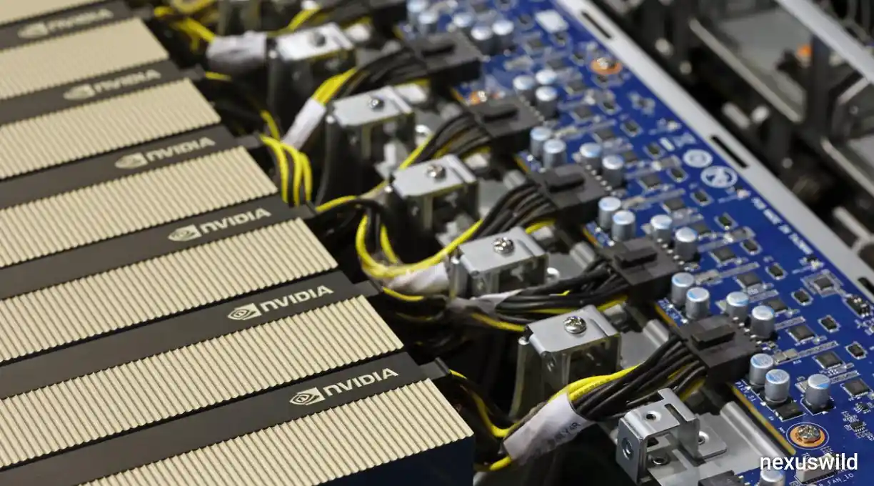
The project is strategically important because advanced packaging has become a stage in the production of high‑performance memory. As AI accelerators become more powerful and data‑centre workloads grow, the ability to manufacture, stack, connect and test high‑bandwidth memory is increasingly important to the performance of computing systems.
Inside the Onyang facility
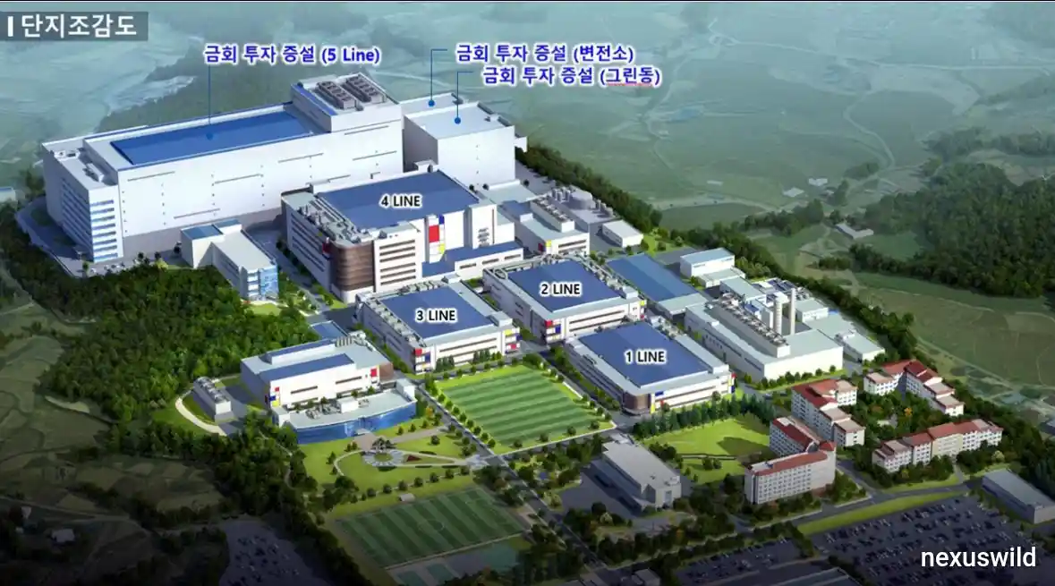
The new facility is planned as a three‑storey production building with approximately 31,000 square metres of cleanroom space. Samsung intends to use the site for HBM production and packaging operations.
The project represents the HBM production line planned for the Onyang campus. It should not be confused with a building containing five separate new lines: the fifth‑line designation refers to the wider campus production plan.
Once the expansion is completed the campus’s total floor area is expected to increase from 270,000 square metres to around 420,000 square metres. The additional space and equipment are intended to support a transformation of Onyang from a site historically associated with semiconductor assembly and testing into a major centre for advanced HBM packaging.
The new line is scheduled to begin operations in June 2028. That target is reportedly around one year earlier than Samsung’s schedule reflecting Samsung’s effort to respond to strong demand for server memory.
The June 2028 date remains a planned target. Actual production ramp‑up will depend on construction progress, equipment installation, process qualification, manufacturing yields and customer validation.
Why advanced packaging has become a bottleneck
HBM is a specialised type of memory designed to provide high data‑transfer bandwidth for processors that handle demanding workloads. It is particularly important in AI accelerators and high‑performance computing systems, where processors need to access volumes of data quickly.
Unlike memory products HBM uses vertically stacked memory dies connected through advanced interconnect technologies. These stacks must be. Packaged with extreme precision. The packaging process affects performance, thermal behaviour, reliability and the ability to manufacture products at commercial scale.
This makes advanced packaging a strategic part of the AI semiconductor supply chain. Increasing wafer production alone does not necessarily translate into an increase in finished HBM supply. Memory dies must also pass through packaging, bonding, testing and qualification processes.
The growing importance of this stage has encouraged memory manufacturers to expand their back‑end production capabilities. Samsung’s Onyang project is designed to increase Samsung’s capacity in this part of the supply chain and strengthen the connection between memory manufacturing and final packaged products.
The ₩46 Trillion Investment Plan
The investment programme has two components.
The first is ₩6 trillion in construction spending for the advanced packaging fab. The second is around 40 trillion ₩ in equipment investment, which is expected to be deployed in stages.
The distinction is important. The 40 trillion ₩ figure is not a payment or the construction cost of the new building. It represents a longer‑term equipment investment programme associated with the Onyang expansion.
Advanced packaging facilities require manufacturing tools for processes such as bonding, thinning, stacking, inspection and testing.
The equipment programme is therefore central to the facility’s production capability.
The scale of the plan also illustrates how capital‑intensive the competition, for AI memory supply has become.
Companies are not simply adding assembly space. They are investing in production systems designed to handle increasingly complex memory architectures and demanding performance requirements.
The timing and order of putting equipment in place will be important. Installing tools in stages can let a manufacturer match capacity increases with product testing, customer needs and the creation of HBM generations.
Samsungs 2027 HBM supply position
The new plant arrives while Samsung says there is demand for its HBM products. On October 29 2026 during its third‑quarter earnings call Samsung said that the planned HBM supply for 2027 was already sold out at the agreed target prices.
The company also said that big customers still asked for supply. This shows that the current customer commitments might be larger than the volume Samsung has set aside. It does not mean that every possible order or future capacity increase is already used up.
The statement matters because HBM customers usually need to plan supply ahead of deployment. AI accelerator makers and big cloud‑computing firms need access to memory parts as they build new generations of servers and data‑centre systems.
Supply agreements can give manufacturers a view of future demand and help them plan investment.. Commitments do not remove execution risk. Suppliers still have to meet specs, quality rules, delivery dates and customer qualification standards.
Samsungs planned capacity growth is therefore closely linked to its effort to turn demand visibility into manufacturing output.
HBM4 and the next generation of AI memory
The HBM market is moving through generations of products that have more bandwidth, more capacity and more technical complexity. Samsung has been working to strengthen its position in this market through its HBM4 lineup and the creation of next‑generation products.
The company also said it sent HBM4E samples and got early feedback from customers. This is a sign of its product‑development plan but it should not be seen as proof that the new Onyang plant will only make HBM4E.
The plant has been described as a modern HBM production and packaging site. Its final product mix will depend on Samsungs manufacturing plan, customer approvals and the needs of memory generations.
The larger goal is to build packaging capacity that can support advanced HBM products as AI accelerators grow. Higher memory bandwidth and better integration can help meet the rising data needs of computing systems.
Competition with SK Hynix and other memory suppliers
Samsungs investment happens while there is competition in the HBM market. SK Hynix has built a role in supplying advanced memory for AI accelerators and Micron is also growing its HBM abilities.
Competition is not decided by how much money is invested. Memory suppliers must deliver products that meet customer performance needs get manufacturing yields keep reliability and grow production at competitive costs.
Advanced packaging is one area where these abilities come together. A maker may have memory fabrication tech but its skill to package and test products quickly can affect how fast it delivers finished HBM modules.
Samsungs Onyang expansion is meant to improve this part of its production system. It also shows an industry trend where semiconductor makers invest in many stages of the value chain to support AI demand.
The competition result will depend on execution. Samsung must show that the new capacity can produce products at the needed performance levels and on time.
The broader ₩144 trillion Chungcheong investment programme
The Onyang HBM plant is one part of a bigger Samsung affiliate investment program across South Koreas Chungcheong region.
The larger plan is ₩144 trillion and includes investments from four Samsung affiliates: Samsung Electronics, Samsung Display, Samsung Electro‑Mechanics and Samsung SDI.
Samsung Electronics provides about ₩60 trillion of the regional plan, including investments linked to its Onyang and Cheonan semiconductor operations. Samsung Display has set about ₩67 trillion for investment while Samsung Electro‑Mechanics and Samsung SDI provide about ₩8 trillion and ₩9 trillion respectively.
The program covers industries, such as advanced semiconductor packaging, display manufacturing, AI server substrates and batteries. It is meant to strengthen the regions system and encourage more investment by suppliers and materials companies.
The ₩144 trillion regional number should not be blamed on the Onyang HBM project. The plants ₩46 trillion campus plan is a separate part of the larger regional investment program.
Government strategy and regional industrial development
The Korean government has put the Chungcheong initiative in the context of a larger effort to spread advanced industrial investment, beyond the countrys main manufacturing hubs.
The groundbreaking on November 12 was one of the projects highlighted in the mega‑project programme. Government officials said that this strategy is meant to encourage investment in semiconductors, advanced materials, displays and other technology‑intensive sectors.
For the region large‑scale projects can create opportunities for construction contractors, equipment suppliers, specialist service providers, research institutions and skilled workers. The impact will depend on how much of the supply chain's developed locally and how effectively smaller companies can participate.
Yonhap reported that the Onyang facility is expected to create about 700 jobs. More jobs may come from construction, equipment installation, maintenance, logistics and supplier activity. The total of indirect jobs will depend on how the project is carried out.
The government also stressed the importance of linking corporate investment to opportunities for local businesses and workers. This will be a test of whether the regional programme delivers wider economic benefits beyond just expanding large‑company production facilities.
Benefits for semiconductor equipment suppliers
The phased equipment programme could create opportunities for companies that work with advanced packaging machinery, precision bonding, inspection, testing and materials processing.
Manufacturers of semiconductor equipment may benefit if Samsung goes ahead with the planned deployment of tools. Suppliers that have technologies could compete for contracts as the project moves from construction into equipment installation and production qualification.
However the ₩40 trillion equipment allocation should not be seen as confirmed revenue for any named supplier. Samsung has not publicly stated that specific companies have secured orders for the programme.
Potential beneficiaries could include international equipment manufacturers.. The final distribution of contracts will depend on technical specifications, procurement decisions, pricing, production requirements and supplier qualification.
Materials companies may also find opportunities as the facility raises its demand for packaging materials and process inputs. The scale of those opportunities will become clearer once Samsung shares details about the production system and supplier network.
The risk of HBM oversupply
The rapid growth of HBM capacity at Samsung, SK Hynix and Micron raises a long‑term question: could supply growth eventually outstrip demand?
The current investment cycle is driven by demand from AI infrastructure developers. Data‑centre operators and AI chip manufacturers need high‑performance memory as they expand computing capacity.
Semiconductor markets are cyclical. Capacity projects take years to finish and investment made during a time of demand can add supply after market conditions change.
If AI infrastructure spending slows if accelerator demand grows slowly than expected or if several manufacturers expand production at the same time the HBM market could face tighter pricing and utilisation conditions later in the decade.
That is a risk scenario, not a confirmed forecast. The outcome will depend on how fast AI's adopted the memory content per accelerator, product transitions, manufacturing yields and how much new capacity is taken up by customers.
Samsungs phased equipment spending may give some flexibility to match investment with market conditions. The company will still need to manage the risk of committing capital before future demand arrives.
What the project means for the AI supply chain
The Onyang expansion shows how important memory packaging is in the AI hardware ecosystem. AI infrastructure relies on a chain of processors, memory, networking equipment, power systems cooling technologies and data‑centre facilities.
HBM holds an important place because it feeds data to advanced processors. Limits in memory production or packaging can affect how how much AI accelerator systems cost.
By expanding its packaging capacity Samsung aims to strengthen its ability to supply a critical component of that ecosystem. The project also strengthens South Korea’s position as a hub for semiconductor manufacturing and technology investment.
For global technology companies extra HBM capacity could eventually provide another supply source.. The practical effect will depend on successful qualification and how fast the facility reaches commercial production.
What investors and industry participants should monitor
Several indicators will show whether Samsung’s investment is turning into market competitiveness.
The first indicator is construction progress toward the June 2028 target. Delays, in building completion, equipment delivery or cleanroom qualification could change the timing of capacity additions.
The second indicator is the pace of advanced equipment installation. The ₩40 trillion programme is planned in phases so the timing and scale of procurement are signs of how fast the campus is expanding.
The third step is customer qualification. New HBM products must meet the performance, reliability and compatibility requirements of AI chip customers. Positive sample feedback is encouraging. Commercial success depends on HBM qualification and sustained delivery.
The fourth step is production yield. Advanced packaging involves processes and the ability to make reliable HBM products at scale will influence the economics of the investment.
Finally market participants must watch AI infrastructure spending and the capacity plans of competing memory suppliers. These factors will help determine whether the market remains supply‑constrained or moves toward a balanced position.
packaging capacity becomes a central AI hardware battleground.
I saw Samsungs November 12 groundbreaking at the Onyang campus. It marks a significant step in South Koreas effort to strengthen its advanced semiconductor manufacturing base. The ₩6 trillion construction project, supported by a ₩40 trillion in phased equipment investment is intended to expand HBM packaging capacity and transform the site into a major production hub.
I see the planned June 2028 operational start places the project within the phase of the global AI infrastructure expansion. Samsungs reported commitment of its 2027 HBM supply volumes underlines the demand pressure that is driving investment across the memory industry.
I believe the long‑term significance of the project will not be measured by the headline investment figure. Construction execution, equipment deployment, HBM qualification, manufacturing yields and market demand will determine how much additional capacity becomes commercially productive.
For Samsung the project is both a capacity expansion and a competitive commitment. For South Korea the project is an element of a broader regional industrial strategy. For the AI supply chain the project is another indication that advanced memory packaging has become a decisive factor, in the race to scale next‑generation computing.
Nexuswild welcomes factual corrections. Email contact@nexuswild.com with evidence and the article URL.