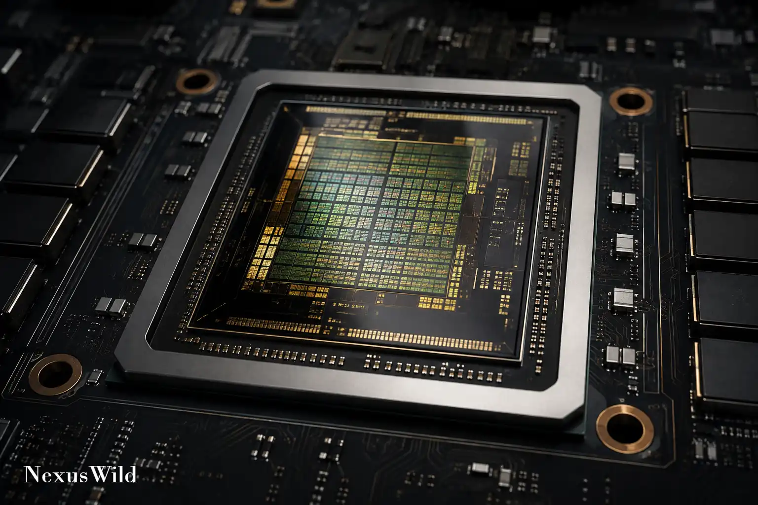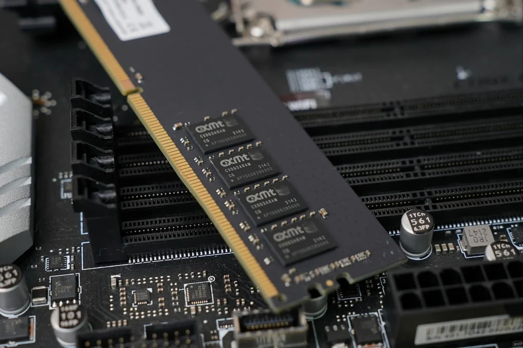

The global semiconductor landscape is witnessing a significant shift as China's leading domestic memory chipmaker officially advances into the next era of integrated circuit manufacturing. On September 20, 2026, during the World Manufacturing Convention held in Hefei, Anhui province, ChangXin Memory Technologies announced that its highly anticipated fifth-generation dynamic random-access memory (DRAM) technology platform has formally entered mass production. The announcement represents a defining milestone for Chinese chip manufacturing, confirming that domestic producers can successfully scale highly advanced memory architectures despite facing stringent international export restrictions on semiconductor manufacturing equipment.
Dynamic random-access memory serves as the critical short-term working memory that powers everything from mobile handsets to high-performance computing centers. Securing a domestic supply of these vital components has been a central pillar of China's broader technological strategy. By commencing volume manufacturing of its latest memory modules, the Hefei-based manufacturer has demonstrated rapid technical progression. The newly mass-produced fifth-generation platform is specifically engineered to deliver more powerful memory chips at a substantially lower cost and with significantly reduced power consumption compared to the company's previous iterations.
The mass production milestone is not merely a laboratory success or a pilot program. The company confirmed that high-density products manufactured on this new platform are already rolling off the assembly lines and being integrated into commercial supply chains. This development ensures that electronics manufacturers operating within the domestic market now have a highly capable, alternative source of supply for the critical components needed to power modern smart devices. As the artificial intelligence revolution continues to drive unprecedented demand for faster and more efficient data storage solutions, the launch of China's latest memory chips stands as a transformative moment for both the regional technology sector and the global semiconductor market.
Mass-Production Details and Manufacturing Scale
The transition from research and development validation to full-scale mass production is widely considered the most difficult hurdle in semiconductor manufacturing. The recent announcement in Hefei confirms that the Chinese manufacturer has successfully cleared this barrier for its fifth-generation node. Moving beyond small-batch testing, the production facilities are now achieving commercial yield rates that make the technology financially viable and highly scalable for broad market distribution.
A key highlight of the mass production phase is the dramatic improvement in manufacturing efficiency. Company executives revealed that the new fifth-generation platform increases the gross die output per silicon wafer by more than fifty percent when compared directly to the fourth-generation manufacturing process. This exponential increase in die-per-wafer output is achieved through advanced structural density, allowing the factory to extract a significantly higher number of functional chips from the exact same raw material footprint. This efficiency gain is crucial for lowering the unit cost of each memory module, allowing the Chinese supplier to compete aggressively on price while maintaining profitability.
The scale of this manufacturing effort reflects years of intense capital investment and operational optimization. While exact facility capacity numbers remain closely guarded, the rapid transition to mass production indicates that the company has secured a stable supply of necessary raw materials, chemicals, and processing tools. To achieve this commercial scale amid ongoing global trade tensions, the manufacturer relied heavily on computer simulation models and direct joint development initiatives with domestic Chinese semiconductor equipment suppliers. By optimizing the production line with locally sourced engineering solutions, the firm has insulated its manufacturing operations from external supply chain shocks.
Furthermore, market research indicates that the manufacturer's revenue and output have surged concurrently with these technological upgrades. In the first half of 2026, the company's revenue increased nearly tenfold compared to the same period in the previous year, successfully turning a profit while expanding its global market footprint. This robust financial performance provides the necessary capital expenditure to maintain continuous mass production and fund the ongoing expansion of fabrication facilities required to meet surging downstream demand.
Breakthrough Chip Technology and Quadruple Patterning
At the core of this manufacturing achievement is a sophisticated engineering workaround that pushes the physical limits of available lithography equipment. The newly mass-produced chips are based on the LPDDR5X standard, a low-power double data rate synchronous dynamic random-access memory protocol specifically optimized for portable electronics. The company unveiled two distinct 24-gigabit product variations built on this fifth-generation platform, both designed to offer fifty percent greater storage capacity than their predecessors while occupying minimal physical space.
The most impressive technical specification of the new platform is its miniaturization. The chipmaker successfully reduced the spacing between the core structures of the memory cells that store digital data, achieving an active-area half-pitch of approximately 11.95 nanometers. In addition, the memory arrays feature a highly advanced capacitor depth-to-width ratio of forty-five to one, ensuring stable electrical performance and reliable data retention even at microscopic scales. Breaking the twelve-nanometer barrier is universally recognized within the semiconductor industry as a marker of leading-edge memory production.
Achieving this 11.95-nanometer density presented a unique challenge. Since 2022, international export controls have restricted Chinese companies from acquiring extreme ultraviolet (EUV) lithography machines, the standard tools used by overseas manufacturers to print ultra-fine circuits. To bypass this limitation, the Chinese manufacturer implemented a highly complex technique known as quadruple patterning.
Quadruple patterning involves using older, more accessible deep ultraviolet lithography machines but repeating the exposure and etching steps multiple times. By carefully overlaying patterns four consecutive times, the engineers can create circuit lines that are significantly finer than the optical resolution limit of a single exposure pass. While quadruple patterning requires extreme precision to align the overlapping layers perfectly, mastering this technique has allowed the Chinese firm to achieve world-class transistor density using standard, unrestricted equipment.
The success of the fifth-generation LPDDR5X mass production also paves the way for future standards. Industry reports confirm that the manufacturer is simultaneously testing next-generation LPDDR6 mobile memory, which promises peak design speeds of up to 12,800 megabits per second. The current mastery of deep ultraviolet multi-patterning ensures that the production lines are mechanically and operationally prepared to handle the upcoming transition to even faster memory protocols.
Commercial Applications and End Users
The commercial deployment of the new 24-gigabit LPDDR5X memory chips is strictly aligned with the demands of the modern consumer electronics and high-performance computing sectors. Memory chips are the unsung engines of the digital economy, and the specifications of this fifth-generation platform make it highly attractive for a wide array of technological applications.
The primary target market for the newly mass-produced chips is the smartphone industry. According to the manufacturer, the new memory modules have already entered the commercial supply chain and are actively supplying major Chinese smartphone manufacturers. These chips are designed specifically for flagship devices, where physical space is at a premium and battery life is a critical selling point. The LPDDR5X standard provides the massive bandwidth necessary to support high-resolution displays, seamless multitasking, and advanced mobile gaming, all while operating on ultra-low power designs that preserve battery longevity. The availability of two different package formats ensures that the chips can be easily integrated into diverse handset designs, including the increasingly popular foldable smartphone category.
Beyond mobile phones, the applications for high-density, low-power memory are rapidly expanding. The rise of artificial intelligence has created an insatiable demand for fast data processing at the edge of the network. The new Chinese memory chips are ideally suited for AI-enabled tablets, smart wearables, and advanced Internet of Things (IoT) hardware. In these devices, the ability to process localized machine learning algorithms without connecting to a cloud server relies entirely on the speed and capacity of the onboard memory.
Furthermore, the automotive sector represents a massive growth opportunity for the newly produced memory modules. Modern smart vehicles require immense computational power to run advanced driver-assistance systems, complex infotainment displays, and real-time navigation processing. The enhanced reliability and dynamic power-saving modes engineered into the fifth-generation platform make these chips highly suitable for the rigorous environments of next-generation digital computational automotive infrastructure.
Strategic Importance for China's Semiconductor Industry
The commencement of mass production for the 11.95-nanometer memory chips carries profound strategic implications for China's broader national technology objectives. For decades, the global semiconductor supply chain has been highly concentrated, with the vast majority of advanced memory production controlled by a handful of international market leaders. The successful launch of this fifth-generation platform signals a definitive shift toward Chinese self-sufficiency in one of the most critical foundational technologies of the twenty-first century.
This milestone is particularly significant given the current geopolitical climate. Over the past several years, foreign governments have imposed sweeping export restrictions on advanced semiconductors, precision manufacturing equipment, and specialized design software to China. These measures were explicitly intended to cap the technological advancement of the Chinese semiconductor industry by cutting off access to next-generation lithography tools. However, the successful implementation of quadruple patterning proves that domestic Chinese chipmakers possess the engineering resilience to innovate around external blockades. By developing localized production processes through computer simulations and domestic equipment partnerships, the manufacturer has effectively neutralized a significant portion of the trade restrictions.
The strategic impact is already reflecting in global market metrics. According to data from industry analysts at Counterpoint Research, the leading Chinese memory chipmaker saw its share of the global dynamic random-access memory market more than double over the past year, rising from four percent in the second quarter of 2025 to ten percent in the second quarter of 2026. This rapid capture of market share demonstrates that domestic consumer electronics companies are enthusiastically adopting homegrown memory solutions to mitigate their own supply chain risks.
Financial analysts project that this trajectory will only accelerate as mass production of the fifth-generation platform scales up. Estimates from Goldman Sachs suggest that the leading domestic manufacturer could supply approximately half of China's total dynamic random-access memory demand by the year 2028. This level of domestic substitution will retain billions of dollars of revenue within the Chinese economy that would have otherwise been spent on imported components. Furthermore, establishing a robust, self-reliant memory sector provides a secure foundation for China's broader ambitions in artificial intelligence, supercomputing, and telecommunications infrastructure.
Impact on the Global Semiconductor Market
While the primary focus of the new mass production is serving domestic demand, the sheer scale of the Chinese electronics industry means that this development will trigger ripple effects across the entire global semiconductor market. The introduction of highly competitive, mass-produced Chinese memory chips fundamentally alters the supply and demand dynamics of the international tech sector.
Currently, the global semiconductor market is experiencing unprecedented demand, driven largely by the explosive growth of generative artificial intelligence and high-performance cloud computing. Data indicates that the global dynamic random-access memory market expanded by fifty-seven percent quarter-over-quarter in recent months. International market leaders have overwhelmingly pivoted their production lines toward high-margin server components to supply massive artificial intelligence data centers. This pivot has inadvertently created a supply bottleneck in the traditional mobile and consumer electronics memory sectors.
The mass production of China's fifth-generation LPDDR5X chips arrives at exactly the right moment to address this global shortage. By supplying massive quantities of high-quality memory to domestic electronics manufacturers, the Chinese chipmaker alleviates pressure on the strained international supply chain. This allows global device manufacturers to secure alternative sources for their component needs, preventing severe price spikes and production delays in the consumer tech industry.
Furthermore, the emergence of a formidable Chinese competitor introduces much-needed diversification into a highly consolidated market. The manufacturer officially stated that its mass production efforts are expected to contribute significantly to the diversification of the global memory market supply chain. Increased competition forces all players in the industry to accelerate their own research and development cycles, ultimately driving down costs and spurring faster technological innovation for consumers worldwide. As the Chinese producer expands its product portfolio, the established international incumbents will face intense pressure to maintain their market dominance, reshaping the competitive landscape for years to come.
Expert Views and Future Manufacturing Challenges
The successful scaling of the 11.95-nanometer process has garnered significant attention from semiconductor analysts and industry experts. Speaking at the World Manufacturing Convention, Luo Xiaodong, a vice president overseeing the marketing center for the Chinese chipmaker, confidently assessed the company's progress. He stated that their process capabilities have now reached a level comparable to the industry's most advanced mass-production nodes. This bold declaration reflects the company's internal confidence in the stability, yield rates, and performance of their quadruple patterning technology.
However, semiconductor manufacturing experts caution that while the current achievement is monumental, maintaining this momentum will present ongoing engineering challenges. The primary concern revolves around the long-term economic viability of multi-patterning techniques. Using deep ultraviolet lithography to perform quadruple patterning requires the silicon wafer to undergo significantly more exposure, etching, and cleaning cycles than a single pass with a restricted extreme ultraviolet machine.
Each additional step in the manufacturing process introduces a new opportunity for microscopic defects, which can negatively impact the final wafer yield. Additionally, increasing the number of processing steps inherently extends the time it takes to complete a single batch of silicon wafers, placing a ceiling on factory throughput. As the industry inevitably moves toward even smaller nodes, such as sub-ten-nanometer architectures, the complexity of multi-patterning will increase exponentially. Analysts note that while the Chinese manufacturer has successfully optimized the process for the current twelve-nanometer generation, pushing the technology to a fifth or sixth patterning pass may eventually yield diminishing economic returns.
Despite these future hurdles, the immediate focus remains on maximizing the output of the current mass-produced platform. Industry experts widely agree that the current generation of memory chips provides more than enough performance density to meet the requirements of modern consumer devices for the foreseeable future. By securing robust yield rates today, the manufacturer generates the crucial capital and engineering experience needed to explore alternative next-generation packaging and materials science breakthroughs tomorrow.
Conclusion
The announcement that China's latest fifth-generation dynamic random-access memory chips have entered full-scale mass production marks a watershed moment in the history of the global semiconductor industry. By achieving an active-area half-pitch of 11.95 nanometers through innovative quadruple patterning techniques, the Chinese manufacturer has successfully circumvented severe international trade restrictions to deliver world-class component density. With the new 24-gigabit LPDDR5X products already supplying major domestic smartphone manufacturers, China has taken a massive and verifiable step toward complete technological self-reliance. As production continues to scale, this breakthrough will not only secure the domestic electronics supply chain but also reshape the competitive dynamics of the international memory market, ensuring that the digital infrastructure of tomorrow is built on a more diverse and resilient foundation.
Further reading and useful links
Reader questions
Frequently asked questions
What breakthrough did ChangXin Memory Technologies announce?
CXMT officially commenced mass production of its fifth-generation DRAM technology platform, featuring 24-gigabit LPDDR5X memory chips built on an 11.95-nanometer process node.
How did CXMT achieve 11.95nm density without EUV lithography?
Due to international export controls on EUV machines, the company utilized quadruple patterning with accessible deep ultraviolet (DUV) lithography tools, repeatedly exposing and etching wafers to surpass optical resolution limits.
Which products are using the new fifth-generation memory chips?
The new 24-gigabit LPDDR5X chips are already actively supplying major domestic Chinese smartphone manufacturers for flagship and foldable handsets, with broader applications across AI edge devices and smart automotive systems.
What is the strategic impact of this milestone for China?
This milestone dramatically accelerates China's semiconductor self-sufficiency, with CXMT's global DRAM market share reaching 10% in mid-2026 and Goldman Sachs projecting domestic producers could meet half of China's DRAM demand by 2028.
Nexuswild welcomes factual corrections. Email [email protected] with evidence and the article URL.