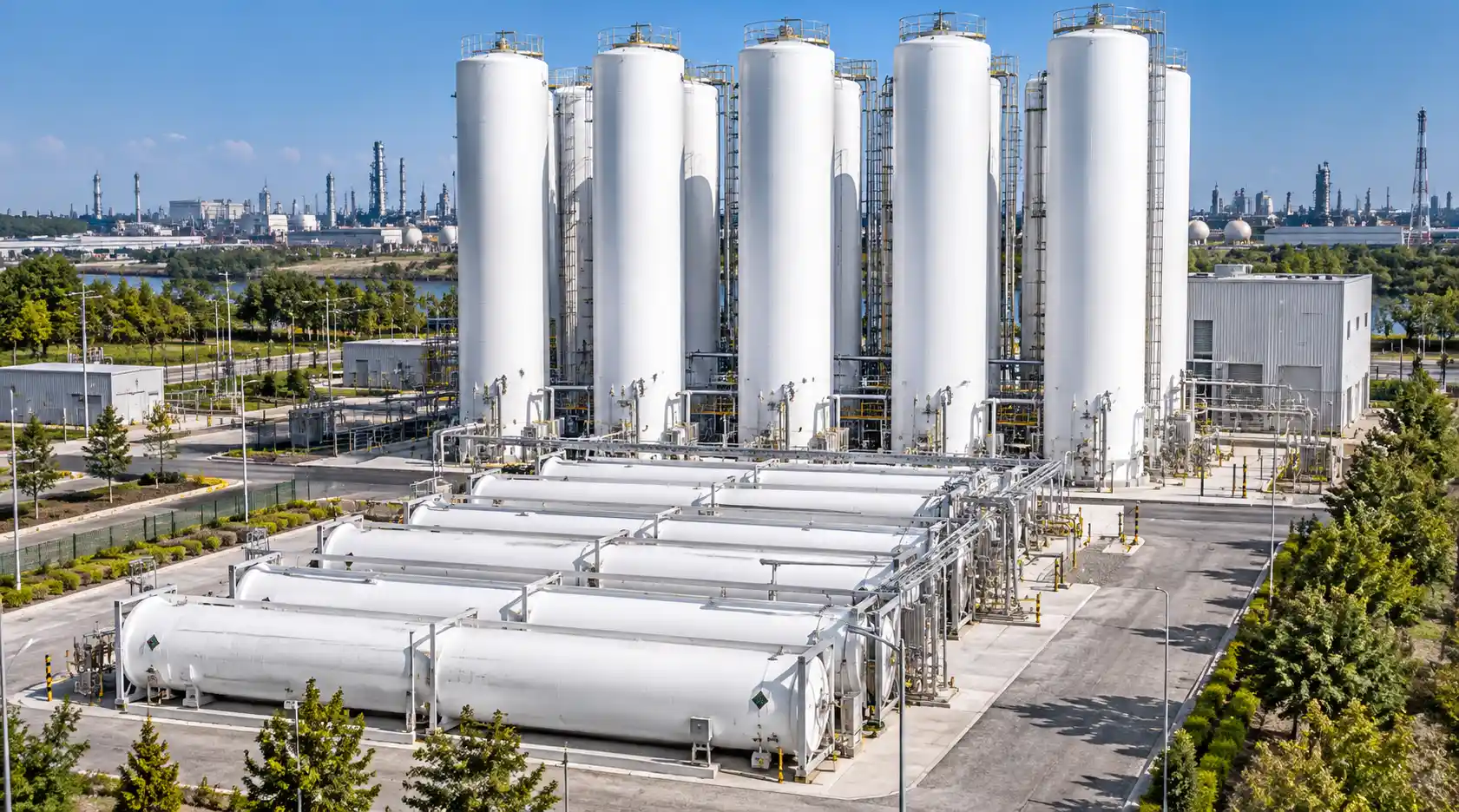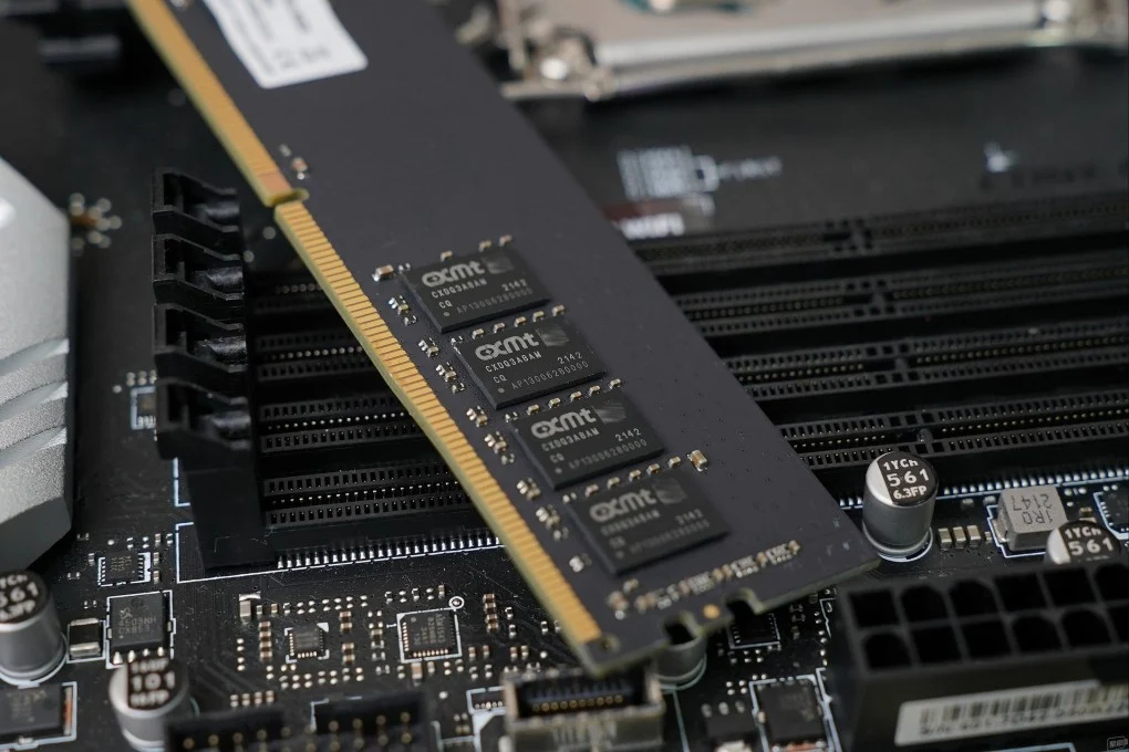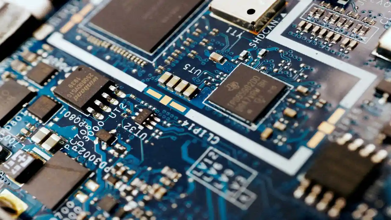

Renesas Electronics’ semiconductor venture with CG Power and Industrial Solutions and Thailand-based Stars Microelectronics has moved into a new operational stage following the start of commercial production at its outsourced semiconductor assembly and test (OSAT) facility in Sanand, Gujarat.
The project is being developed through CG Semi Private Limited, a joint venture in which CG Power holds approximately 92.3%, while Renesas and Stars Microelectronics hold approximately 6.8% and 0.9%, respectively. The venture has committed more than ₹7,600 crore over five years to establish semiconductor packaging and testing capabilities in Sanand. (Renesas)
The first facility, known as G1, began commercial production on 4 July 2026 after progressing through equipment installation, process stabilisation, workforce training, customer qualification and quality-readiness activities. The facility has a stated peak capacity of approximately 300 million semiconductor units per year. (Yahoo Finance)
Recent reporting now describes the project as entering an optimisation phase. In practical manufacturing terms, this refers to the work required after commissioning and commercial start-up to improve production performance, stabilise processes, raise yields and increase throughput toward the facility's designed operating capability. (The Financial Express)
The development is significant because the Sanand project is focused on the assembly, packaging and testing stages of semiconductor manufacturing rather than wafer fabrication. These downstream processes are essential for converting semiconductor dies into tested, packaged devices ready for use in electronic products.
Renesas Chip Venture Update
The Sanand project originated from a partnership announced by CG Power and Industrial Solutions, Renesas Electronics and Stars Microelectronics.
Under the original agreement, Renesas was to provide semiconductor technology and expertise, while Stars Microelectronics would contribute OSAT technology for legacy packages as well as training and enablement. CG Power was positioned as the majority shareholder and project developer. (Renesas)
The joint venture planned a manufacturing facility in Sanand capable of handling a broad range of semiconductor packages. The originally announced product scope included established packages such as QFN and QFP, as well as more advanced packaging formats including FC BGA and FC CSP. The venture identified automotive, consumer electronics, industrial applications and 5G among its target sectors. (Renesas)
The project subsequently progressed from construction and pilot operations to commercial production.
The G1 facility was inaugurated in August 2025. According to government information, the facility was designed to handle approximately 0.5 million units per day, while the larger G2 facility was planned to scale the overall operation substantially. (Press Information Bureau)
On 4 July 2026, CG Semi announced the commencement of commercial production at G1 in Sanand. The announcement followed a period involving equipment installation, process stabilisation, workforce training, customer qualification and preparation for quality requirements. (Yahoo Finance)
The Indian government also confirmed the beginning of commercial chip-packaging production at the facility. The Prime Minister's Office said the Sanand facility represented an important addition to India's semiconductor manufacturing ecosystem. (Press Information Bureau)
This means the project has moved beyond simply building semiconductor infrastructure. The immediate focus is now on making the installed manufacturing system operate consistently at commercial standards while increasing production efficiency.
What the Optimisation Phase Means
The term optimisation phase should not be interpreted as a separate manufacturing technology or as evidence of a restructuring programme unless the companies specifically announce such a programme.
For the Sanand venture, the available evidence points instead toward the normal operational progression of a newly commissioned semiconductor packaging facility.
Before a new OSAT operation reaches stable commercial output, manufacturing teams must establish repeatable processes across equipment, materials, testing systems, packaging operations, quality controls and trained personnel.
CG Semi's commercial-production announcement specifically referred to:
- Equipment installation
- Process stabilisation
- Workforce training
- Customer qualification
- Quality readiness
These activities provide a useful factual basis for understanding the project's optimisation stage. (Yahoo Finance)
In semiconductor manufacturing, yield is particularly important. Yield broadly measures the proportion of devices that successfully meet specified manufacturing and quality requirements. Improving yield can allow a facility to obtain more saleable output from the same underlying production resources.
Throughput is another important measure. It describes how much material or how many units can move successfully through a manufacturing process over a given period.
Therefore, when reporting describes G1 as working to improve yield and throughput toward its designed capacity, the optimisation phase can be understood as a period of operational learning and refinement rather than an announcement that the plant is being rebuilt or fundamentally restructured. (The Financial Express)
The distinction is important because a facility can have a stated peak capacity while its actual output during early commercial operations is lower. Reaching a published maximum generally requires stable processes, qualified products, trained employees, reliable equipment performance and sufficient customer demand.
Technology and Production Capabilities
CG Semi's Sanand project is an OSAT operation.
OSAT facilities perform downstream semiconductor activities including assembly, packaging and testing. Unlike a wafer fabrication plant, an OSAT facility does not manufacture semiconductor wafers from raw silicon through front-end transistor fabrication.
Instead, semiconductor dies are processed through packaging and testing operations so that they can subsequently be integrated into electronic systems.
The Sanand venture's original technology plan included several package families.
QFN and QFP
QFN and QFP are established semiconductor package formats used across a wide range of electronic products.
Their inclusion gives the facility exposure to established semiconductor packaging requirements rather than restricting it to a single emerging application.
FC BGA and FC CSP
The project also identified more advanced packaging formats, including flip-chip ball grid array (FC BGA) and flip-chip chip-scale package (FC CSP). These technologies can support different requirements for electrical connectivity, physical dimensions and performance.
The availability of multiple packaging technologies is important because semiconductor customers have different requirements depending on the chip design and the end application.
The joint venture's announced target industries include automotive, consumer, industrial and 5G applications. (Renesas)
Recent information from CG Semi also describes the Sanand operation as supporting automotive, consumer electronics, industrial manufacturing and 5G-related markets. (LinkedIn)
The facility is therefore not designed around a single chip category. Its role is to provide packaging and testing capacity that can serve different semiconductor products and end markets.
G1 and the Next Expansion Stage
The first commercial facility, G1, has a stated peak capacity of approximately 300 million units annually, equivalent to about 0.5 million units per day based on the project's stated operating figures. (Yahoo Finance)
The broader Sanand project includes a second facility, G2, which is under development.
Government information published in 2025 stated that G2 was planned to eventually reach approximately 14.5 million units per day. (Press Information Bureau)
More recent reporting has also described G2 as the facility that will provide a major increase in overall packaging capacity as the project expands. (The Financial Express)
This two-stage structure is important to understanding the current optimisation period.
G1 is already in commercial operation. Its immediate task is to establish stable production and progressively improve utilisation and manufacturing performance.
G2 represents the larger capacity expansion. Its construction and subsequent equipment installation will create additional manufacturing capability beyond the initial G1 operation.
Consequently, the current phase should not be described as if the full planned Sanand capacity is already operating. The project's published future capacity remains dependent on the completion and ramp-up of the additional infrastructure.
Investment and Business Strategy
The Sanand semiconductor venture involves an investment commitment of approximately ₹7,600 crore over five years.
Renesas originally stated that the investment would be financed through a combination of subsidies, equity and potential bank borrowings. (Renesas)
The project's financing structure also involves public semiconductor-support programmes. Earlier government information said CG Semi had received approval for fiscal support of up to approximately ₹3,501 crore, subject to the applicable agreement and conditions. (LinkedIn)
For Renesas, the venture provides a route to participate directly in semiconductor packaging operations in India while maintaining a relatively small equity ownership position.
Renesas contributes technology and semiconductor expertise to the venture, while CG Power is the majority partner and Stars Microelectronics provides OSAT experience and technology support. (Renesas)
This structure gives the project a combination of local manufacturing ownership, semiconductor technology expertise and established packaging experience.
The business significance extends beyond the physical plant.
Renesas is a major supplier of semiconductor solutions used across automotive, industrial and other electronics applications. Its current corporate strategy also places significant emphasis on embedded processing, digitalisation, intelligence at the edge and AI infrastructure. Renesas' 2026 investor materials separately identify Software-Defined Vehicle, Embedded Processing & Digitalization Strategy, Intelligence at the Edge, and AI Infra & Compute among its strategic areas. (Renesas)
However, the Sanand OSAT facility should not automatically be described as an AI-chip manufacturing plant. The officially announced Sanand product scope covers semiconductor packaging and testing across several application areas. Specific AI-related production allocations should be reported only when confirmed by the companies.
Renesas' Broader Semiconductor Strategy
The Sanand venture forms part of Renesas' broader effort to strengthen its semiconductor business across automotive and industrial markets while expanding its capabilities around emerging computing requirements.
Renesas' financial disclosures show that the company continues to monitor demand conditions and operational performance across its semiconductor business.
For the second quarter of 2026, Renesas reported consolidated revenue of ¥405.3 billion, gross profit of ¥235.3 billion, operating profit of ¥132.7 billion and EBITDA of ¥154.3 billion on a non-GAAP basis. For the first six months of 2026, revenue was ¥777.6 billion and operating profit was ¥258.2 billion on the same basis. (Renesas)
These are Renesas-wide figures and should not be treated as financial results for CG Semi or the Sanand facility itself.
That distinction matters because the joint venture is a separate project with its own investment, manufacturing ramp and customer relationships.
The available public information does not establish a standalone revenue or profit figure for the Sanand facility at its current early commercial stage.
Impact on the Semiconductor Supply Chain
The Sanand venture is strategically relevant because semiconductor supply chains extend beyond chip design and wafer fabrication.
Packaging and testing are essential stages between semiconductor production and the final electronic product.
A chip may be successfully fabricated but still requires appropriate packaging, electrical connections, testing and quality verification before it can be incorporated into an electronic system.
The Sanand facility therefore adds capacity to a part of the semiconductor value chain that India has historically depended heavily on overseas suppliers for.
The Indian government has described the facility as part of a broader effort to develop capabilities spanning semiconductor design, fabrication, packaging and testing. (Press Information Bureau)
For CG Semi, increasing production at Sanand could also create opportunities to serve customers from India and international markets.
The project has already demonstrated an international dimension. Recent reporting said the facility had begun commercial shipments of assembled semiconductor devices to Malaysia for customers connected with Renesas before the formal July commercial-production inauguration. (Moneycontrol)
This illustrates an important feature of OSAT manufacturing: the factory's customers and end markets do not have to be located in the same country as the packaging operation.
A Sanand facility can therefore participate in international semiconductor supply chains while manufacturing in India.
Manufacturing Efficiency and Capacity Utilisation
The transition from pilot activity to commercial manufacturing creates a new set of operational priorities.
At this stage, several factors become important:
- Yield improvement: Manufacturers seek to increase the percentage of packaged devices that meet required specifications.
- Throughput improvement: Production systems need to process more units without compromising quality.
- Equipment utilisation: Installed manufacturing equipment needs to operate reliably and efficiently.
- Process stability: Packaging and testing processes must produce consistent results over repeated production cycles.
- Quality qualification: Customers need confidence that the packaged devices meet their technical and reliability requirements.
- Workforce capability: Employees must be trained to operate specialised semiconductor manufacturing and testing systems.
CG Semi's own announcement confirms that process stabilisation, training, customer qualification and quality readiness took place before commercial production. (Yahoo Finance)
The optimisation stage can therefore be viewed as a continuation of those activities.
It is also why published peak capacity should not be confused with immediate utilisation. A facility can be engineered for hundreds of millions of units annually while requiring time to ramp production toward that theoretical or designed maximum.
Market and Industry Challenges
The semiconductor sector remains sensitive to changes in electronics demand, inventory cycles, capital expenditure, production economics and customer ordering patterns.
For a new OSAT facility, another important consideration is the balance between available capacity and customer demand.
Packaging capacity only becomes economically productive when qualified semiconductor products and customer orders are available to use it.
CG Power Chairman Vellayan Subbiah said in August 2026 that the global semiconductor packaging market remained supply-constrained and that capacity was being directed toward AI-related applications. His comments were reported by ET Electronics. (ETElectronics.com)
Those comments provide one industry perspective on the market environment, but they should not be interpreted as a guarantee of future demand for the Sanand project.
The project also faces the normal operational challenges associated with scaling semiconductor manufacturing.
These include maintaining consistent quality, improving yields, training specialised workers, qualifying additional products, ensuring equipment availability and managing the economics of packaging services.
As G2 comes online, the scale of the operation will increase substantially. That makes process control and customer diversification increasingly important to the project's long-term utilisation.
Company and Government Views
Government officials have publicly highlighted the Sanand facility's role in developing India's semiconductor ecosystem.
At the July 2026 inauguration, Prime Minister Narendra Modi described the beginning of commercial chip packaging at the CG Semi facility as part of India's effort to build a broader semiconductor value chain. (Press Information Bureau)
The Union Ministry of Electronics and Information Technology also said that the commencement of commercial production marked an important development for India's semiconductor sector. (Press Information Bureau)
From the company's side, the project's structure reflects a division of responsibilities among the three partners.
CG Power brings the majority ownership and local manufacturing platform.
Renesas contributes semiconductor technology and expertise.
Stars Microelectronics contributes OSAT technology, including legacy-package expertise, as well as training and enablement. (Renesas)
The combination is designed to create a manufacturing operation capable of supporting multiple semiconductor applications rather than a facility dedicated to a single product line.
Why the Optimisation Stage Matters
The most important change at Sanand is the transition from project construction to repeatable commercial manufacturing.
Building a semiconductor facility is only one part of establishing semiconductor capacity. The manufacturing process must subsequently demonstrate reliable quality, stable production and the ability to serve customer requirements consistently.
The G1 facility has already completed the key preparatory stages identified by CG Semi, including equipment installation, process stabilisation, workforce training, customer qualification and quality readiness. (Yahoo Finance)
The next challenge is to improve the efficiency and consistency of those operations while increasing output.
This is particularly relevant because the Sanand project has ambitious long-term capacity plans.
The first plant has a stated annual capacity of about 300 million units, while the broader two-facility project is designed to reach much higher production levels. (Yahoo Finance)
The performance of G1 therefore provides an important foundation for the expansion of G2.
Successful process learning at the first facility can help establish manufacturing procedures, workforce expertise and quality systems that can be applied as the wider operation grows.
The Road Ahead for CG Semi
The immediate priority for the Sanand venture is operational ramp-up.
G1 is already in commercial production, while G2 remains part of the project's expansion programme.
As the facilities develop, the company will need to balance three requirements: production scale, manufacturing quality and customer demand.
The project's original product roadmap covers both established and advanced semiconductor packaging technologies. (Renesas)
Its target markets include automotive, consumer, industrial and 5G applications, providing a broad potential customer base. (Renesas)
At the same time, the company must continue qualifying products and maintaining manufacturing standards as production volumes increase.
The future capacity figures should therefore be viewed as planned or designed capability rather than current output.
The same distinction applies to future revenue expectations. Public reports have discussed the potential financial contribution of the semiconductor business at scale, but those figures should not be treated as current revenue from the G1 facility unless the company reports them directly.
Conclusion
Renesas' semiconductor venture with CG Power and Stars Microelectronics has entered an important operational stage at its Sanand, Gujarat, OSAT facility.
The project's G1 facility began commercial production on 4 July 2026 after completing equipment installation, process stabilisation, workforce training, customer qualification and quality-readiness activities. It has a stated peak capacity of approximately 300 million semiconductor units annually. (Yahoo Finance)
The term optimisation phase describes the next step in that manufacturing journey: improving process stability, yield, throughput and utilisation as the facility moves deeper into commercial operations. It should not automatically be interpreted as a restructuring exercise or a new expansion announcement.
The wider project represents an investment of approximately ₹7,600 crore over five years and includes a second facility, G2, that is intended to substantially expand packaging capacity. (Renesas)
For Renesas, the venture provides a manufacturing and packaging presence in India supported by local industrial capability and OSAT expertise. For CG Power and Stars Microelectronics, it creates a platform for expanding semiconductor assembly and testing operations.
The significance of the project ultimately depends on execution: stable production, competitive manufacturing economics, customer qualification, quality performance and the successful scaling of additional capacity.
For now, the verified development is clear: CG Semi has moved from facility commissioning into commercial production, and the Sanand operation is now focused on establishing and improving its manufacturing performance as the broader project expands.
Further reading and useful links
Nexuswild welcomes factual corrections. Email [email protected] with evidence and the article URL.