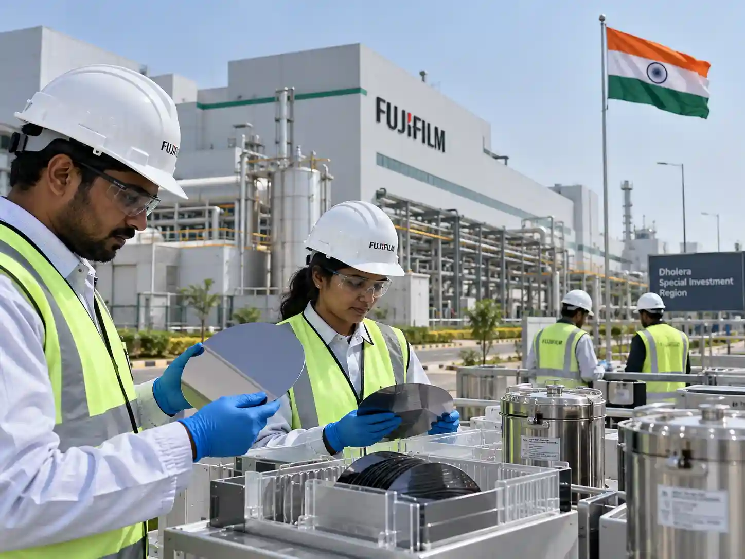

The industrial landscape of Gujarat is undergoing a structural transformation as global chemical and technology giants establish deep roots in the region. In a move that anchors the country's chemical supply chains for high-tech electronics, Japanese multinational Fujifilm announced a planned investment of approximately ₹800 crore to construct a dedicated semiconductor materials manufacturing facility. Situated within the Dholera Special Investment Region (DSIR), the project is designed to support the sprawling domestic semiconductor fabrication ecosystem taking shape under major national industrial initiatives.
The formalization of the project follows a strategic Memorandum of Understanding (MoU) signed with Tata Electronics. Rather than operating as an isolated manufacturing unit, Fujifilm's upcoming plant is tailored to act as a vital localized material supplier for Tata Electronics' multi-billion-dollar chip fabrication plant in Dholera. By establishing local production lines for high-purity chemicals and specialty inputs, the investment addresses one of the most persistent structural bottlenecks in India’s nascent semiconductor sector: heavy reliance on imported raw materials.
Fujifilm’s ₹800 Crore Investment Phasing
The planned capital expenditure of roughly ₹800 crore (approximately $83 million) will be deployed in strategic phases. This phased rollout allows Fujifilm to align its production capacity directly with the construction milestones of the primary fabrication facility it serves.
The agreement builds upon earlier exploratory frameworks, including a preliminary MoU signed between FUJIFILM India and the Gujarat State Electronics Mission during a regional industrial conference. With formal partnership agreements now established with major domestic fabrication entities, the project moves from initial planning toward land allocation, facility design, and eventual engineering execution. Company executives note that the initiative will also involve close collaboration with local Indian chemical manufacturers, providing technology transfer, quality assurance standards, and process know-how to build a dependable domestic vendor base.
What the Dholera Plant Will Produce
Semiconductor manufacturing is widely considered one of the most chemically intensive manufacturing processes on Earth. The Dholera facility will focus on producing advanced chemical formulations that dictate the precision of microscopic circuitry on silicon wafers.
According to technical disclosures from Fujifilm’s Electronic Materials division, the product portfolio for the regional supply chain will include photoresists and photolithography-related materials, which are light-sensitive chemicals used to transfer circuit patterns onto silicon wafers. The plant will also manufacture chemical-mechanical planarization (CMP) slurries and post-CMP cleaners - specialized fluids and abrasives used to flatten and polish wafer surfaces at an atomic level between layer depositions.
Additionally, the facility is slated to produce thin-film materials, photosensitive insulating materials such as polyimides marketed under the ZEMATES brand, and Wave Control Mosaic functional materials utilized in color filters for advanced image sensors. These inputs are foundational for producing integrated circuits that serve automotive systems, consumer electronics, computing architecture, and artificial intelligence infrastructure.
Why Semiconductor Materials Matter
To understand the strategic gravity of Fujifilm's investment, one must look inside a modern semiconductor fabrication plant, commonly known as a "fab." Tata Electronics is constructing a massive 300-millimeter (12-inch) wafer fabrication facility in Dholera designed for a capacity of 50,000 wafers per month, spanning mature and advanced technology nodes from 28nm to 110nm.
Even the most advanced fabrication machinery cannot produce a single working chip without ultra-pure chemical inputs. Impurities measured in parts per billion can ruin an entire batch of silicon wafers worth millions of dollars. By producing these sensitive materials locally, the Dholera supply chain avoids the logistical vulnerabilities, customs delays, and high shipping costs associated with importing reactive chemicals from overseas processing hubs. Local production ensures that fabrication lines maintain uninterrupted operational continuity.
Dholera’s Growing Semiconductor Ecosystem
The choice of Dholera as the host site for both chip fabrication and supporting chemical manufacturing is the result of deliberate infrastructure planning. Designated as a Special Investment Region (SIR), Dholera has been engineered from the ground up with robust utilities, dedicated industrial zoning, bulk water supplies, reliable high-capacity power grids, and multimodal connectivity tied to the Delhi-Mumbai Industrial Corridor (DMIC).
The convergence of fabrication units, packaging facilities, and specialty chemical suppliers in one geographic cluster mirrors successful semiconductor clusters globally, such as those in Taiwan, South Korea, and the United States. Analysts point out that creating this localized ecosystem reduces transit risks for hazardous chemical precursors, which require specialized temperature-controlled logistics and strict regulatory clearances.
Impact on India’s Chip Supply Chain
India’s broader industrial strategy hinges on moving up the global value chain. While national policies have successfully attracted high-profile commitments for semiconductor fabrication, building a sustainable domestic electronics sector requires domesticating the supporting ecosystem.
Without local chemical suppliers, packaging houses, and equipment maintenance providers, a domestic fab remains vulnerable to external trade disruptions. Fujifilm’s investment directly targets this vulnerability. By embedding advanced chemical formulation expertise within Gujarat, the project creates a technical bridge between international specialty manufacturing standards and local industrial capabilities.
Industry and Leadership Perspectives
Corporate leadership from both participating entities have underscored the collaborative nature of the venture. Randhir Thakur, CEO and Managing Director of Tata Electronics, emphasized that building a resilient manufacturing base requires robust supply chain integration.
"Our strategic partnership with Fujifilm marks an important step in strengthening the semiconductor materials supply chain for our Dholera Fab," Thakur stated. "By combining Fujifilm's expertise in advanced semiconductor materials with Tata Electronics' vision of creating a robust manufacturing base, we are enhancing supply chain resilience for our global customers and accelerating ecosystem development."
From the corporate headquarters in Japan, Teiichi Goto, President and CEO of FUJIFILM Holdings Corporation, highlighted the strategic significance of the Indian market. Goto noted that Fujifilm positions its electronic materials business as a core engine for corporate growth, recognizing India's rapid technological expansion as an ideal environment for long-term capital deployment. Tetsuya Iwasaki, General Manager of Fujifilm's Electronic Materials Business Division, added that the company is eager to introduce its proprietary formulation technologies to support India's vision of advanced technological self-reliance.
Challenges and Operational Horizons
Despite the positive momentum, establishing a high-purity chemical manufacturing plant involves rigorous technical hurdles. Semiconductor-grade materials demand stringent cleanroom environments, zero-defect quality control systems, and complex waste management protocols to handle hazardous effluents safely.
Furthermore, translating complex chemical formulations into consistent commercial output requires intensive workforce training and close coordination with local environmental regulators. As the project transitions from memorandum signing to physical construction and subsequent pilot testing, engineers will need to ensure that local output matches the exact quality benchmarks required by international chipmakers.
Conclusion
Fujifilm’s planned ₹800 crore investment in Dholera represents a pragmatic and essential component of India's evolving semiconductor roadmap. By moving beyond assembly and fabrication to tackle the complex domain of high-purity process chemicals and photoresists, the initiative tackles supply chain dependencies at their root. As infrastructure development progresses across the Dholera Special Investment Region, this materials facility will serve as a foundational building block for a self-sustaining domestic electronics manufacturing economy.
Further reading and useful links
Reader questions
Frequently asked questions
How much is Fujifilm investing in the Dholera semiconductor project?
Fujifilm is planning an investment of approximately ₹800 crore (around $83 million) to construct a semiconductor materials manufacturing facility in Dholera, Gujarat.
Which company is Fujifilm partnering with for this venture?
Fujifilm has signed a strategic Memorandum of Understanding (MoU) with Tata Electronics to act as a localized material supplier for Tata's Dholera chip fabrication plant.
What products will the Dholera facility manufacture?
The plant will produce high-purity semiconductor materials including photoresists, chemical-mechanical planarization (CMP) slurries, post-CMP cleaners, thin-film materials, and photosensitive insulating materials.
Why is local semiconductor material manufacturing important for India?
Local production eliminates the heavy reliance on imported raw materials, reduces logistical and customs vulnerabilities, and ensures uninterrupted operational continuity for domestic fabrication units like Tata Electronics.
Nexuswild welcomes factual corrections. Email [email protected] with evidence and the article URL.